
Carbon-Based Electronic Materials: Carbon Nanotubes
Carbon nanotubes—often called CNTs—are one of those materials you just can’t ignore anymore if you work with electronics or materials science. I’ve been around long enough to see a fair share of promising materials come and go, but CNTs have held their ground. They’re tiny, sure, but their performance in real-world use speaks louder than size.
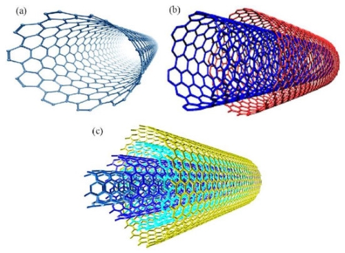
Fig 1. Structure of (a) a single-walled carbon nanotube (SWCNT), (b) a double-walled carbon nanotube (DWCNT), and (c) a multi-walled carbon nanotube (MWCNT).
The Structure behind the Hype
Now, let’s keep it simple. A carbon nanotube is like a rolled-up sheet of graphene. Picture a chicken wire rolled into a straw, and you’re not far off. These tubes are sealed at both ends, and they can come in different forms—sawtooth, armchair, and spiral. That last one has something we call “chirality,” which can affect how it conducts electricity.
Most of the carbon atoms in these tubes are sp² hybridized, meaning they share electrons in a way that makes the structure pretty stable and tough. But not every bond is perfect. There are spots where atoms bend or twist out of line, and you get what we call topological defects. Think dents and bulges on a smooth pipe. These affect how the electrons move through the material.
Single-walled tubes are usually more chemically quiet. They don’t react as much with other substances. Multi-walled ones, on the other hand, are more active—lots of carboxyl groups and other reactive sites show up on their surfaces. That’s handy if you want to attach something to them, but it can also complicate things if you’re looking for consistent performance.
Electrical Properties That Matter
Let’s not bury the lead: carbon nanotubes conduct electricity very well. Some types act like metals. Others behave more like semiconductors. It depends on how the atoms are arranged. We use a simple notation—(n, m)—to describe that layout. If 2n + m happens to be a multiple of 3, then you’ve got a metallic nanotube. Otherwise, it’s a semiconductor.
Now, that might sound too textbook, but here’s the practical bit: if you’re building circuits or looking for high-speed performance, you can tailor what kind of CNT you use based on this (n, m) rule.
Conductivity also changes with tube size. Tubes smaller than 6 nanometers act like quantum wires—they’re fast and efficient. Bigger than that, and performance drops off a bit. In some rare setups, like ultra-narrow 0.7 nm tubes, researchers have found signs of superconductivity—though you’d need temperatures near absolute zero for that. Still, it shows potential.
Real-World Applications
CNTs aren’t just interesting on paper. They’re already doing work out there.
--EFETs (Electron Field Emission Transistors)
CNTs are great at handling current and heat. That’s why they’ve been used in field emission displays—like the screens in older picture tubes or micro-lasers. Devices built with CNTs tend to last longer and run more efficiently because the tubes help emit electrons more evenly.
--Electronic Sensors
One of the most useful traits of CNTs is their sensitivity. They pick up on small changes in their environment—temperature, pressure, chemical exposure—and they do it fast. That makes them ideal for building sensors. These can be used in flexible electronics, wearables, and even in rough environments like manufacturing lines or high-heat systems.
A case worth mentioning: researchers made a sensor using cobalt-manganese oxide with CNTs. The combination gave better readings and lasted longer, which is exactly what engineers want in sensor tech.
Solar Cells
CNTs have been added to some types of solar cells to improve performance. The idea is simple—get better conductivity, reduce energy loss, and maybe extend lifespan. While there’s not a mountain of public data yet, trials show promise. Especially in cells where the goal is to be thin, flexible, and still efficient.
Challenges That Still Need Work
As good as CNTs are, they’re not perfect. Manufacturing them in large quantities while keeping their structure consistent is still a problem. Impurities and uneven surfaces make it tough to use them in high-precision electronics. Also, aligning them just right—so the electricity flows the way you want—is tricky. It’s one thing to grow a CNT in the lab. It’s another to integrate it neatly into a chip or a circuit board.
Another issue is how CNTs interact with other materials. Sometimes they bond too much, other times too little. Surface chemistry needs careful handling. That’s why post-processing is a big deal—cleaning, sorting, and functionalizing the tubes to fit the application.
Still, with steady work and the right techniques, many of these problems are getting solved. Slowly, but surely. For more semiconductor materials and applications, please check Stanford Electronics.
FAQs
Q1: Are carbon nanotubes always conductive?
No. Only certain types are metallic. Others behave like semiconductors, depending on their atomic structure.
Q2: Can carbon nanotubes be used in consumer electronics today?
Yes, but mostly in niche areas like sensors and experimental flexible displays. Large-scale use is still developing.
Q3: Do carbon nanotubes have any health or safety concerns?
Some studies suggest inhalation could pose risks, similar to asbestos. Proper handling in lab and manufacturing settings is essential.
Reference:
[1] Ferrier, D.C.; Honeychurch, K.C. Carbon Nanotube (CNT)-Based Biosensors. Biosensors 2021, 11, 486. https://doi.org/10.3390/bios11120486


 Powder for Li-ion Battery Cathodes")
