
Two-Dimensional (2D) Semiconductors: The New Wave of Electronics
Introduction to 2D Semiconductors
Two-dimensional (2D) semiconductors are a revolutionary frontier in material science, with properties that extend beyond those of conventional bulk materials. From their names, one realizes that they are atomically thin—ranging from a single layer of atoms—and this gives them remarkable mechanical, electronic, optical, and thermal properties. In contrast to conventional bulk semiconductors such as silicon, 2D semiconductors tend to have direct band gaps, intense quantum confinement, high carrier mobility, and optoelectronic tunability.
The most well-known of the materials are graphene, one atomic layer of honeycomb-arranged carbon atoms. But while graphene has terrific conductivity, it has no band gap, so it has no role in conventional semiconductor devices. This limitation has been the spur to much research into other 2D materials with intrinsic semiconducting character, such as transition metal dichalcogenides (TMDs)—molybdenum disulfide (MoS₂), tungsten diselenide (WSe₂), and many others.
These materials are now the subject of thousands of research articles annually. To provide an example, over 7,000 articles on 2D semiconductors were published as of 2022, indicating the rapid growth and essential role in future nanoelectronics, flexible electronics, and quantum computing technology.
[1]
Applications of 2D Semiconductors
2D semiconductors are being investigated for their ability to revolutionize many electronic and optoelectronic applications.
1. Field-Effect Transistors (FETs)
MoS₂ FETs have already demonstrated amazing performance at nanoscales. Unlike silicon, which suffers from short-channel effects when scaled below 10 nm, monolayer MoS₂ has exquisite electrostatic control. In a remarkable report by Radisavljevic et al. (2011), a MoS₂ transistor exhibited an on/off current ratio of over 10⁸ with a subthreshold swing of ~74 mV/decade and demonstrated its potential in low-power, high-performance logic circuits.
2. Flexible and Wearable Electronics
The atomically thin nature of 2D semiconductors allows them to be electronically functional but mechanically flexible. This makes them able to be integrated into wearable health monitors, roll-up displays, and foldable smartphones. For instance, researchers at the University of Wisconsin produced a flexible array of transistors using MoS₂ that was found to function even when subjected to 5% strain.
3. Photodetectors and Solar Cells
Due to their high light-matter interactions, many 2D semiconductors are good photodetectors. WSe₂ and MoTe₂ photodetectors have already shown high photoresponsivity (over 10³ A/W in some reports), rendering them useful for ultrathin imaging purposes. Also, the stacking of two dissimilar 2D materials renders van der Waals heterostructures feasible, allowing precise band alignment for photovoltaic devices without the limitation of lattice matching. Theoretical efficiency limits of such cells have been predicted to be over 20%.
4. Quantum Computing and Neuromorphic Devices
Room-temperature excitonic effects and spin-valley coupling are demonstrated by 2D semiconductors and have tremendous potential for quantum information technology. Quantum light emission from single defect states has been reported in certain TMDs, a key prerequisite for photonic qubits. In neuromorphic computing, 2D memristors that use layers like MoS₂ or h-BN mimic synaptic action and can be scaled down to atomic thicknesses.
Development of 2D Semiconductors
The route from discovery to device-quality 2D semiconductors has been one of great advances in synthesis, integration, and comprehension of their properties.
1. Material Synthesis
Early studies employed mechanical exfoliation ("Scotch tape method") to obtain monolayers of materials like MoS₂. While acceptable for proof-of-principle demonstrations, the process is not scalable. Chemical vapor deposition (CVD) has since emerged as a scalable procedure, producing wafer-scale monolayers of WS₂ and MoS₂. In 2021, MIT scientists grew a 4-inch continuous MoS₂ monolayer by CVD, a move toward industrial integration.
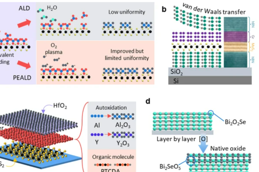
2. Heterostructure Engineering
One of the most powerful aspects of 2D materials is the possibility of stacking different layers without concern for lattice mismatch, creating van der Waals heterostructures. These can be designed to uniquely achieve new band alignments and functionality. For example, layer-stacking MoS₂ with graphene produces ultrafast tunneling transistors, whereas layer-stacking WSe₂ with MoTe₂ is capable of creating photovoltaic devices with high open-circuit voltages.
3. Challenges and Future Directions
While promising, 2D semiconductors also pose daunting challenges:
- Contact Resistance: Low-resistance, stable metal contacts remain difficult to achieve due to Fermi level pinning and interfacial defects.
- Scalability and Uniformity: Films deposited by CVD tend to have grain boundaries, vacancies, and non-uniform thickness, which degrades performance.
- Device Integration: Integrating 2D semiconductors with existing CMOS infrastructure demands new fabrication approaches.
- However, constant innovations in interface engineering, plasma processing, and dopant control are gradually addressing these issues. TSMC's 2D Semiconductor Foundry Program with research partners is a step to standardize processes and accelerate adoption into commercial chip manufacturing.
Conclusion
2D semiconductors have evolved in electronics revolution. With outstanding properties and growing industrial interest, these atomically thin materials promise to transform computing, sensing, and energy conversion. While obstacles still abound, ongoing breakthroughs in synthesis and integration point toward a clear path. For more advanced semiconductors, please check Stanford Electronics.
References:
1. Radisavljevic, B. et al. "Single-layer MoS₂ transistors." Nature Nanotechnology, 6, 147–150 (2011).
2. Jariwala, D. et al. "Emerging Device Applications for Semiconducting Two-Dimensional Transition Metal Dichalcogenides." ACS Nano, 8(2), 1102–1120 (2014).
3. Li, M. et al. "Wafer-Scale MoS₂ Monolayers via CVD Growth." Nature Materials, 20, 1357–1363 (2021).
4. Li, Y. et al. "2D Materials for Neuromorphic and Quantum Devices." Advanced Materials, 33, 2003610 (2021).
5. "Two-dimensional semiconductors: from fundamental physics to emerging applications." Nature Electronics, 5, 70–84 (2022).
6. Huang, X., Liu, C. & Zhou, P. 2D semiconductors for specific electronic applications: from device to system. npj 2D Mater Appl 6, 51 (2022). https://doi.org/10.1038/s41699-022-00327-3


 Powder for Li-ion Battery Cathodes")
