
Chemical Vapor Deposition Defined
What Is Chemical Vapor Deposition (CVD)
Chemical Vapor Deposition refers to a chemical vapor-phase process employed for the deposition of thin solid films on a substrate. In CVD, volatile chemical precursors are made to react or decompose on the surface of a heated substrate to form a desired material film. Unlike physical deposition processes based on physical transfer of material, CVD is chemically reaction-based to form highly adhesive and uniform films.
CVD is widely used in semiconductor, optics, and coating production because it can coat conformal high-purity films onto complex three-dimensional substrates. Silicon dioxide (SiO₂) and silicon nitride (Si₃N₄) are common materials coated using CVD, alongside titanium nitride (TiN), aluminum oxide (Al₂O₃), tungsten (W), and other metals and oxides used in electronics, MEMS, and photovoltaics.
[1]
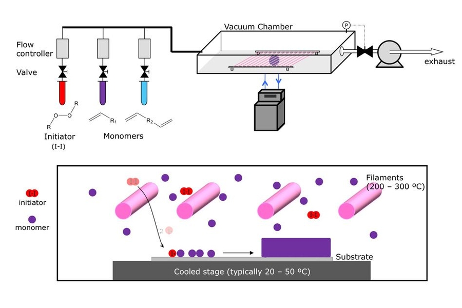
How It Works
The process of CVD is usually carried out in a number of steps:
1. Introduction of Precursors:
Fluctuating chemical substances are introduced into a reaction chamber. The precursor gases used are selected based on the composition of film required. Silane (SiH₄), for example, is utilized in depositing silicon-containing films.
2. Transport to Substrate
Precursors are transported in carrier gases, most commonly nitrogen or hydrogen, to the substrate surface. Substrate is commonly preheated to a certain temperature, usually somewhere between 200°C and over 1000°C, depending on the material and the reaction type.
3. Film Formation by Chemical Reaction:
After the precursor molecules reach the substrate, they are subjected to chemical processes such as decomposition, reduction, or oxidation. The reaction leaves a solid film on the surface of the substrate and byproducts are pumped out in the form of gases.
4. Exhaust of Byproducts:
Byproducts of the reaction, being primarily gaseous, are pumped from the chamber at regular intervals using a vacuum or gas flow system in an attempt to aid efficiency and purity of the process.
The outcome is a conformal, thin, and uniform film that is able to cover complex geometries, e.g., high-aspect-ratio trenches, vias, and other 3D features.
Types of Chemical Vapor Deposition Systems
CVD technology has developed into various types, each applicable for certain materials and processes. Some common ones are:
1. Atmospheric Pressure CVD (APCVD):
Runs at room atmospheric pressure. APCVD is typically applied in bulk industrial coatings with intermediate uniformity requirements, e.g., protective coating or glass coating.
2. Low-Pressure CVD (LPCVD):
In vacuum to reduce unwanted gas-phase reactions and for better uniformity. LPCVD finds vast use in semiconductor fabrication for depositing SiO₂, Si₃N₄, and polysilicon films on wafers.
3. Plasma-Enhanced CVD (PECVD):
Utilizes plasma to enhance chemical reactions with lower substrate temperatures. PECVD can be applied for heat-sensitive substrates and is generally used for thin dielectric films, passivation layers, and MEMS devices.
4. Metal-Organic CVD (MOCVD):
Uses metal-organic precursors in compound semiconductor deposition such as GaN, InP, and AlGaAs. MOCVD is significant in LEDs, laser diodes, and power devices.
5. Atomic Layer Deposition (ALD):
A highly accurate CVD method in which precursors are added successively in an autorestrictive reaction to build atomic-level thickness control and improved conformality over intricate structures.
Applications of Chemical Vapor Deposition
Versatility of CVD has made it an essential part of numerous high-tech and industrial processes:
1. Semiconductors and Electronics:
CVD provides dielectric films, barrier films, conductive films, and semiconductor materials for sensors, ICs, and MEMS. For instance, CVD-deposited titanium nitride (TiN) is employed as a diffusion barrier in copper interconnects to avoid metal migration and improve the reliability of devices.
2. Photovoltaics:
Thin-film solar cells make extensive use of CVD to deposit CdTe or amorphous silicon layers for better light absorption and efficiency.
3. Protective and Decorative Coatings:
Wear-resistant coating, anti-reflective film, and corrosion-resistant coating can be deposited by CVD on glass, metal, and tool substrates.
4. LED and Optoelectronic Devices:
Compound semiconductors grown by MOCVD such as GaN form the foundation of high-efficiency and long-lifetime laser diodes and high-brightness LEDs.
5. Advanced Materials and 3D Structures:
CVD can deposit material onto high-aspect-ratio structures, nanotubes, and 3D architectures that are of critical relevance to next-generation memory devices, sensors, and energy storage devices.
Conclusion
Chemical Vapor Deposition is a support technology to the discipline of materials engineering today, providing high-purity, accurate films for electronics, energy, and industry. With deposition chemistry, temperature, and atmosphere control, CVD provides pure, uniform, conformal coatings on complex substrates. CVD enables innovation from semiconductor devices to solar cells that see efficiency, reliability, and performance. For more details, please check Stanford Electronics.
Frequently Asked Questions
Q1: What are the advantages of CVD over other deposition methods?
CVD offers greater conformality, purity, and uniformity, even on complex 3D surfaces, and is therefore better for high-precision applications than PVD or spin-coating.
Q2: Will CVD deposit metals and insulators?
Yes. Depending on precursor chemistry, CVD will deposit metals (tungsten, copper), oxides, nitrides, and compound semiconductors and is therefore extremely versatile.
Q3: Are there temperature limitations for CVD?
There are several CVD processes for accepting temperature sensitivity. For example, PECVD and ALD coat lower temperatures when the substrate is temperature sensitive, but LPCVD and APCVD require increased temperatures to have the best film quality.
Q4: What industries are most reliant on CVD?
The most reliant industries on CVD are semiconductors, photovoltaics, LEDs, MEMS devices, aerospace coatings, and tool manufacturing.
Reference:
[1] Chandler, D. L. (2025, June 19). Explained: Chemical vapor deposition. MIT News. Retrieved October 20, 2025, from https://news.mit.edu/2015/explained-chemical-vapor-deposition-0619


 Powder for Li-ion Battery Cathodes")
