Everything about Doped Crystals and Semiconductor Materials
Modern electronics and photonics owe a significant portion of its advancement to doped crystals and semiconductor materials. Right from high-speed transistors to sophisticated laser systems, these materials are the backbone to technologies that make our lives meaningful. It is imperative for scientists, engineers, and hobbyists to comprehend their properties, the process of doping, and the function of semiconductors.

What Are Doped Crystals?
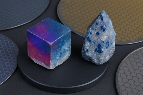
Crystals are solid materials whose atoms occur in a highly regular, repetitive arrangement of setting. Pure crystals, such as silicon or sapphire, have known electronic, optical, and mechanical properties. Pure crystals may not be sufficient for application in most uses because their inherent electrical conductivity or optical property may be insufficient.
This is where doping occurs. Doping is the intentional incorporation of trace amounts of foreign atoms, termed dopants, into a crystal lattice with the purpose of modifying its physical or chemical properties. The dopants occupy positions within the lattice by substituting host atoms or occupying interstitial positions, thereby altering the crystal's behavior.
For example, in laser crystals like Nd:YAG (Neodymium-doped Yttrium Aluminum Garnet), neodymium ions replace part of the yttrium ions in the crystal lattice. This replacement enables the crystal to emit coherent laser light when it is pumped by a pump source. Similarly, in scintillator crystals, doping can enhance the efficiency of luminescence, enabling better radiation detection in medical imaging or in high-energy physics.
The doping process is very controlled. Even minute quantities of dopants—parts per million—can change a crystal's electronic, optical, or magnetic properties significantly. Based on the application, the dopant and concentration are tailored to deliver the desired performance.
Types of Doped Crystals
Doped crystals can broadly be classified based on their primary application:
1. Optically Active Crystals: These include materials like Nd:YAG, Er:YAG, and Ti:sapphire. Energy levels in the dopants in the crystals are suitable for laser fluorescence or emission. Such materials find widespread application in laser systems for industrial, medical, and scientific use.
2. Electrically Active Crystals: Usually semiconductors in which doping alters the concentration of charge carriers. Examples are silicon doped with phosphorus (n-type) or boron (p-type). This form of doping is fundamental to transistors, diodes, and integrated circuits.
3.Magnetically Active Crystals: Rare-earth-doped crystals can have better magnetic properties, helpful in high-performance permanent magnets or magneto-optical devices.
4. Nonlinear Optical Crystals: Doping can be utilized to increase the phase matching or wavelength conversion efficiency of nonlinear optical processes that are important in frequency doubling or optical parametric oscillation.
Semiconductor Materials
Semiconductors form a unique class of materials whose electrical behavior lies midway between conductors and insulators. Their conductivity is highly sensitive to impurities, temperature, and illumination, making them very suitable for electronic and optoelectronic applications.
--Intrinsic vs. Extrinsic Semiconductors
• Intrinsic Semiconductors: These are undoped materials, typically silicon or germanium, that contain an equal number of electrons and holes. They possess an average amount of conductivity under normal conditions.
• Extrinsic Semiconductors: Doped with impurities to increase conductivity. Adding pentavalent atoms like phosphorus to silicon creates an n-type semiconductor with an excess of electrons, whereas trivalent atoms like boron create a p-type semiconductor with an excess of holes. The combination of n-type and p-type regions is required to create diodes, transistors, and photovoltaic cells.
--Common Semiconductor Materials
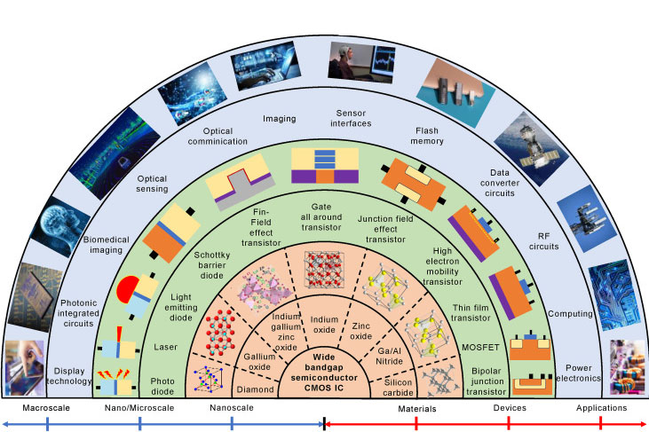
1. Silicon (Si): Widely used semiconductor, especially in microelectronics and solar cells. Stable, available, and thoroughly characterized, it sets the industry standard.
2. Gallium Arsenide (GaAs): Offers higher electron mobility than silicon, making it ideal for high-frequency and optoelectronic applications.
3. Indium Phosphide (InP) and Gallium Nitride (GaN): Both wide-bandgap semiconductors are key to LEDs, laser diodes, and power electronics.
4. Silicon Carbide (SiC) and Diamond: Due to their very high breakdown voltage and high thermal conductivity, these materials are well suited for applications under extreme conditions.
Doping Techniques for Semiconductors
The dopants are introduced into the semiconductors in a variety of ways:
• Ion Implantation: High-energy ions are accelerated and implanted on the semiconductor surface with precisely controlled dopant depth and concentration.
• Diffusion: The semiconductor is heated at elevated temperatures and exposed to a dopant source so that atoms diffuse into the crystal lattice.
• Molecular Beam Epitaxy (MBE) and Chemical Vapor Deposition (CVD): Advanced techniques utilized in the production of layered semiconductor structures with doped profiles, necessary for modern optoelectronic devices.
Applications of Doped Crystals and Semiconductors
Applications are diverse and widespread:
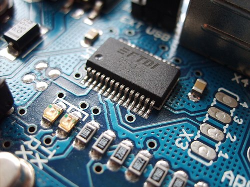
• Electronics: Transistors, diodes, integrated circuits, and sensors rely on precise doping to function at their best.
• Photonics: Lasers, LEDs, and optical amplifiers require doped crystals for emission modulation.
• Energy: Solar cells convert the sunlight into electricity with the help of doped semiconductors to form the charge carriers.
• Medical Devices: Doped scintillation crystals improve imaging devices such as PET and CT scanners.
• High-Power Devices: GaN and SiC semiconductors regulate high currents and voltages in automotive and industrial processes.
Conclusion
Doped crystals and semiconductors are the foundations of modern technology. With careful control of impurities and crystal structures, scientists can determine electrical, optical, and magnetic properties with unprecendented precision. From powering our devices to enabling state-of-the-art medical imaging and lasers, these materials keep driving the world forward. Understanding their mechanisms, types, and uses not only illuminates current technologies but also inspires future technologies. For more information, please check Stanford Electronics.
Frequently Asked Questions
1. What is a doped crystal?
A doped crystal is a pure crystal intentionally modified by adding small amounts of foreign elements called dopants. This changes certain properties—such as optical, electrical, or structural—without significantly altering the crystal’s overall structure.
2. Why are crystals doped?
Doping allows scientists and engineers to “tune” a material’s properties. Pure crystals may lack specific characteristics, but introducing dopants can enhance conductivity, luminescence, or other functional traits for targeted applications.
3. Does doping affect the crystal’s charge?
No. While doping changes electrical behavior, the crystal remains electrically neutral. For example, in a p-type semiconductor, positive “holes” do not create a net charge in the material.
4. What are common dopants?
The type of dopant depends on the desired effect. Typical dopants include transition metals, rare-earth elements, or other atoms chosen to modify optical, electronic, or structural properties.


