
List of Sputtering Targets for Semiconductor Applications
Sputtering targets are essential consumable components in the manufacture of semiconductors. They influence the final composition of the thin film in semiconductors. Below is an extensive list of the primary components in sputtering targets that function in the manufacture of semiconductors.
Why Sputtering Targets Are Important to Semiconductor Manufacturing
Physical Vapor Deposition (PVD) using sputtering has found application in the deposition of conductive, barrier, seed, dielectric, and functional films onto silicon wafers. In this process, highly energetic ions are bombarded onto a solid target, resulting in the ejection of atoms that deposit onto the silicon wafer to create a thin film. There appears to be an intrinsic relation between the purity of the thin film produced and that of the target.
Even trace elements of a part per million level in advanced technology semiconductors can lead to reduced resistivity in thin films, electromigration, or defects. Consequently, the purity level of semiconductor-grade sputtering targets needs to be 99.99% (4N) to 99.9999% (6N), close to theoretical densification, and preferably with a crystalline orientation. All these parameters help promote consistency in erosion rates and wafer consistency.
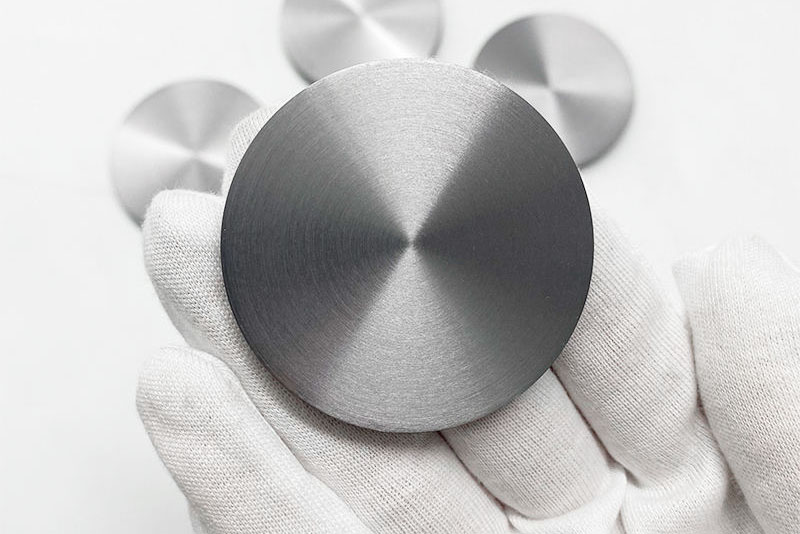
Aluminum (Al) Sputtering Targets
Aluminum had long been the prevailing material for interconnect in integrated circuits and is currently being applied in mature nodes, power components, and analog ICs. Aluminum sputtering targets are characterized by low resistivity, strong adhesive properties to silicon dioxide, and high process stability.
In semiconductor devices, aluminum is doped with a small quantity of copper or silicon to make Al-Cu or Al-Si. The aluminum targets in IC technology have a minimum purity of 5N. Copper has mostly replaced aluminum in latest logic devices. However, aluminum targets are of high importance in MEMS technology and power electronics. They are still in use in the drivers of display units.
Copper (Cu) Sputtering Targets
Copper sputtering targets are very important in semiconductor interconnect technology because copper has a low electrical resistivity and a high electromigration resistance. Copper films of high purity can support high speed and low power consumption, which are very important in advanced logic and memory technology.
Copper targets for semiconductor purposes demand a purity level of 5N to 6N, with low levels of oxygens to avoid resistivity drift and oxidation of the copper films. Copper targets are mostly used for seed layers before electroplating for the process of damascene memory. The grain size and orientation of copper targets determine step coverages and vias or trenches continuity.
Titanium (Ti) and Titanium Alloys Target Material
Titanium sputtering targets have applications as adhesion layers and barrier layers in semiconductor devices. Titanium has a good affinity for both silicon and silicon dioxide. This helps to provide good adhesion and keep metals from diffusing into the lower layers.
In actual application, titanium targets are utilized for the deposition of thin films for the purpose of contact metallization, diffusion barriers, and gate arrangements. Titanium nitride (TiN), usually deposited by the reactive sputtering process using titanium targets, is utilized for its good diffusion barrier properties and moderately good conductivity.
Titanium targets for semiconductors are required to have high densities and proper oxygen composition for achieving uniformity and reproducibility for films deposited by these targets.
Tantalum and Tantalum Compound Targets
Tantalum sputtering targets play an important role in diffusion barrier films, especially in copper interconnects. Tantalum and tantalum nitride (TaN) films prevent copper diffusion into dielectrics, thus ensuring reliability.
Tantalum targets provide a superior level of chemical stability, melting point, and adhesive strength. In modern semiconductor technology, the Ta/TaN stack is adopted in vias and interconnections in order to provide improved electromigration resistance. A target with a higher purity level (4N5–5N) and a fine-grain microstructure is necessary for the target material in order to provide smooth deposition and stable sputter yields.
Tungsten Targets Sputtering Targets
Tungsten sputtering targets are major components of contact plugs, vias, and gate electrodes, particularly in Logs and memory chips. The high melting point of tungsten and its low resistivity in thin films as well as its stability at high temperatures qualify it for high temperature processes.
In semiconductor device technology, the target material used in combination with CVD and ALD processes is tungsten. Sputtered films of tungsten offer excellent step coverage and low contact resistivity. It is important to achieve a high target density and grain structure for reducing particles and stable sputtering due to the brittle nature of tungsten.
Barrier and Liner Materials Targeted
Aside from the basic metals, there are other materials utilized for sputtering targets in the deposition of barrier and liner layers. Chromium (Cr) sputtering targets have niche uses for adhesion and diffusion-related purposes. Molybdenum (Mo) sputtering targets have good conductivity and stability for use in semiconductors and displays.
Such materials are chosen depending on their resistance to diffusion, electrical property, and compatibility with other layers. Semiconductor-grade barrier targets demand strict control of composition in order to maintain uniformity in performance.
Dielectric and Oxide Sputtering Targets
The use of oxide sputtering targets is growing with the increasing complexity of devices. The most commonly used targets include silicon dioxide (SiO₂), aluminum oxide (Al₂O₃), hafnium dioxide (HfO₂), and ITO.
Specifically, Hafnium oxide targets have a prime application in high-k dielectric films in advanced logic technology as a substitute for the conventional SiO2 barrier in order to control the leakage current. There is a need for high uniformity of the chemical composition of these targets in order to maintain a certain dielectric constant and threshold voltage. The ITO targets have a prime application in semiconductor-based display technology as a transparent conductive coating.
How to Select
A compromise of various characteristics of the target material, its purity, density, grain structure, or price has to be taken into consideration while selecting targets for sputtering. For instance, targets of high purity minimize the possibility of target-borne contamination but incur higher costs of materials.
A fine or homogeneous grain structure helps to enhance stability during sputtering while restraining arcs, while targets of near-density close
In volume production of semiconductors, bonded targets where the material for sputtering is attached to a supporting metal plate may be preferable. Target life, erosion rates, and availability for existing PVD equipment can all be important factors in determining the overall cost effectiveness of the process.
Conclusion
Sputtering targets are basic materials used in the semiconductor processing industry and directly affect the quality of thin films and the manufacturing yields of semiconductor devices. Various targets are used for different purposes, including aluminum and copper interconnect targets, tantalum diffusion barrier targets, tungsten contact targets, and oxide dielectric targets. For more details, please check Stanford Electronics.


 Powder for Li-ion Battery Cathodes")
