
The Perovskite Playbook: Properties to Applications
Perovskite materials have changed the course of materials science in the last ten years, enthalling scientists with their distinctive structure, excellent optoelectronic features, and multifaceted applications ranging from solar cells to X-ray detectors.
Initially discovered as a naturally occurring mineral, perovskite now describes an extensive range of materials with the generic formula ABX₃, which have been shown to surpass conventional semiconductors in most fields.
This article discusses the in-depth information on the perovskite structure, properties and diverse technological applications from examples and findings of recent research.
1. Structure of Perovskite
The perovskite crystal structure was first observed in the mineral calcium titanate (CaTiO₃), discovered in 1839. Today, "perovskite" broadly refers to any material with the ABX₃ structure, where:
- A-site cation: A large monovalent or divalent cation such as methylammonium (CH₃NH₃⁺, MA⁺), formamidinium (FA⁺), or cesium (Cs⁺), occupying the corners of the cubic lattice.
- B-site cation: A smaller divalent or trivalent metal ion like lead (Pb²⁺), tin (Sn²⁺), or bismuth (Bi³⁺) at the body center.
- X-site anion: Typically a halide such as iodide (I⁻), bromide (Br⁻), or chloride (Cl⁻), forming octahedra with the B-site cation.
This configuration creates a highly symmetric, flexible lattice that can be manipulated chemically to tune material properties. Depending on the ionic radius and bonding environment, the perovskite structure can also appear in distorted, layered, or reduced-dimensional forms, such as:
- 2D perovskites: e.g., (PEA)₂PbI₄ (PEA = phenylethylammonium)
- 1D perovskites: e.g., chain-like structures useful for stability
- 0D perovskites: isolated clusters, used in quantum dots
The ability to customize A, B, and X sites allows for the design of materials with tailored bandgaps, improved stability, and reduced toxicity.
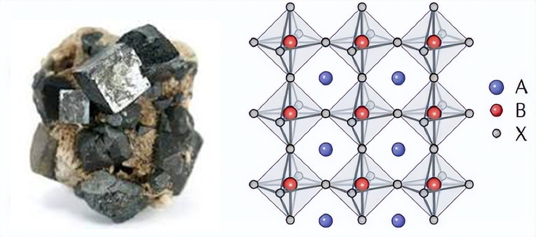
Fig. 1 Structure of Perovskite
2. Key Properties of Perovskite Materials
Perovskites are remarkable due to their combination of excellent optical, electronic, and structural properties—several of which outperform conventional materials such as silicon.
2.1. Tunable Bandgap
The bandgap of perovskite materials can be adjusted from 1.2 eV to 2.3 eV, making them ideal for diverse optoelectronic applications.
- MAPbI₃ (methylammonium lead iodide): ~1.55 eV, optimal for single-junction solar cells.
- CsPbBr₃: ~2.3 eV, suitable for light-emitting diodes.
- Mixed-halide perovskites (e.g., MAPb(BrₓI₁₋ₓ)₃): Bandgap tunable by adjusting halide ratio.
2.2. Strong Light Absorption
Perovskites have a high absorption coefficient (≥10⁵ cm⁻¹), enabling them to absorb most sunlight within a few hundred nanometers of thickness. This results in lightweight, flexible, and cost-efficient photovoltaic devices.
2.3. Balanced Charge Carrier Mobility
Perovskites support both electrons and holes with relatively high and balanced mobility (typically 10⁻¹ to 10 cm²/V·s). This is crucial for efficient charge extraction and minimal recombination.
2.4. Long Carrier Lifetime and Diffusion Length
Carrier diffusion lengths often exceed 1 μm, even in polycrystalline films. For example:
- MAPbI₃: carrier lifetime ~100–1000 ns, diffusion length >1 μm
- FA-based perovskites: can exceed 10 μm with optimized passivation
2.5. Defect Tolerance
Unlike silicon, perovskites can maintain high performance despite structural defects, as many defects form shallow trap states rather than deep recombination centers.
3. Applications of Perovskite Materials
Perovskite materials are now a cornerstone in several cutting-edge technologies:
3.1. Solar Cells
Perovskite solar cells (PSCs) have made spectacular progress since 2009, when their efficiency was just 3.8%. As of 2023, lab-scale devices have reached 26.1% certified power conversion efficiency (PCE), rivaling monocrystalline silicon.
- Tandem solar cells: Combining perovskites with silicon has yielded efficiencies over 33%, surpassing the single-junction Shockley-Queisser limit.
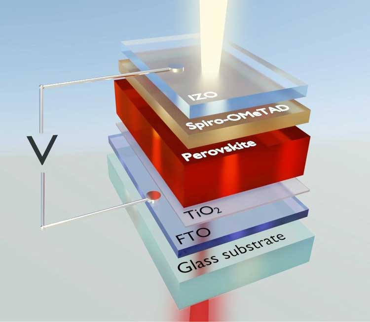
Fig. 2 Perovskite solar cells
3.2. Light-Emitting Diodes (LEDs)
Perovskite LEDs (PeLEDs) are attractive for their pure color emission and high quantum efficiency:
- External quantum efficiencies (EQE): Exceeding 20% in green and red wavelengths.
- Color tunability: Through halide composition and dimensional control.
3.3. Photodetectors and X-ray Imaging
Perovskites like MAPbI₃ and CsPbBr₃ exhibit excellent photoconductive gain and low detection limits. They have been used in:
- X-ray detectors with detection limits below 1 μGyair/s, suitable for medical imaging.
- UV-visible photodetectors with fast response times and high sensitivity.
3.4. Transistors and Lasers
Due to their balanced carrier transport and defect tolerance, perovskites are being explored for:
- Thin-film transistors (TFTs)
- Microlasers and nanolasers, especially using 2D and 0D structures for tight emission control.
4. Challenges and Future Directions
Despite impressive progress, commercial deployment faces two major challenges:
4.1. Lead Toxicity
Most high-performance perovskites contain lead (Pb²⁺), raising environmental and health concerns. Solutions include:
- Lead-free alternatives: Sn²⁺ (tin), Bi³⁺ (bismuth), and Ge²⁺ (germanium)
- Double perovskites: e.g., Cs₂AgBiBr₆, a promising stable and less toxic material
However, these often suffer from lower performance compared to lead-based analogs.
4.2. Stability Issues
Perovskites degrade under humidity, heat, and UV exposure. Strategies to address this include:
- Surface passivation: Use of bulky organic cations or additives (e.g., phenethylammonium)
- Encapsulation: Polymer or glass coatings to isolate from the environment
- Compositional engineering: Incorporating FA⁺ or Cs⁺ improves thermal and phase stability
Some devices have now passed the IEC 61215 qualification test, indicating progress toward long-term operational stability.
Conclusion
Perovskites are perhaps the most exciting frontier in modern materials science. Their new structure provides unmatched control of optoelectronic function, and their runaway performance gains promise commercial application in solar energy, display technologies, and radiation detection. For more semiconductor materials, please check Stanford Electronics.


 Powder for Li-ion Battery Cathodes")
