A Beginner's Guide to Semiconductor Crystals
Semiconductor crystals are at the heart of almost every modern electronic device. From the smartphone in your pocket to the solar panels on rooftops, these materials make modern technology possible. Yet, for those new to the field, the concept of semiconductor crystals can seem abstract or overly technical. We’ll break down the fundamentals, explain how these crystals are formed, and explore the most commonly used semiconductor materials today.
![]()
What Are Semiconductor Crystals?
Semiconductors are materials that fall between conductors, like copper, and insulators, like glass. They do not contain free-moving electrons under normal circumstances, unlike conductors. However, as compared to insulators, the conductivity of semiconductor crystals is not absolute—it can be changed, by heat, light, or chemical doping, to fit specific technological purposes.
The Structure of Semiconductor Crystals
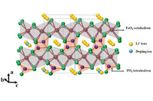
Microscopically, semiconductor crystals consist of a repeating periodic lattice. It is due to this crystalline structure that the material gets its unique electrical properties. The atoms of a semiconductor crystal are bonded in a rigid covalent bond in a pure state, producing a periodic and stable lattice.
This is not merely a question of beauty; it really defines the manner in which electrons travel through the material. If energy is provided, electrons can shift between the valence band and the conduction band, allowing regulated electrical current. This is the operation of virtually all electronic devices, diodes, and transistors.
Why Crystalline Order Matters
The purity and structural consistency of the crystal have a dramatic effect on device performance. Crystal lattice defects, such as dislocations or vacancies, have the potential to trap electrons or impede their flow, reducing efficiency. This is why semiconductor firms invest so heavily in growing high-quality, defect-free crystals.
How Are Semiconductor Crystals Made?
It takes both science and art to form a semiconductor crystal. It can be done a variety of ways, each with its own advantage depending on the intended application.
The Czochralski Method
The most common technique is the Czochralski (CZ) method. In this, a small seed crystal is immersed in molten semiconductor material, typically silicon. Slowly drawing the seed up while it is rotating, melt atoms will adhere to it to form a large single crystal of cylindrical shape. The method produces high-purity crystals for applications in microelectronics.
The Bridgman-Stockbarger Method
Another method is the Bridgman method, where molten semiconductor material cools very gradually inside a vessel. As it cools, one crystal develops at the end of the vessel, gradually enveloping it. This method is widely used in compound semiconductors like gallium arsenide.
Advanced Techniques: MBE and MOCVD
For more advanced applications, like Molecular Beam Epitaxy (MBE) and Metal-Organic Chemical Vapor Deposition (MOCVD), are utilized. These technologies allow for atomic layering with high accuracy, creating ultrathin crystalline films with highly controlled doping. They have significant uses in such devices as high-speed transistors, LEDs, and laser diodes.
Related reading: How Do Single Crystals Grow
What Are The Most Common Semiconductor Materials?
Not all semiconductor crystals are the same. Each material has characteristics that are tailored to specific applications.
Silicon: The Workhorse
Silicon (Si) is the most widely used semiconductor material. Abundant, relatively inexpensive, and chemically inert, silicon is the basis of today's electronics industry. It's ideally suited for integrated circuits, microchips, and solar cells.
Germanium: The Early Pioneer
Germanium (Ge) was one of the first semiconductors used in electronics, in the form of early transistors. Less common today because of its cost and lower thermal stability compared with silicon, germanium continues to be used in specialty applications such as high-speed electronics and infrared optics.
Compound Semiconductors: GaAs and InP
Indium phosphide (InP) and gallium arsenide (GaAs) are some examples of compound semiconductors. Compound semiconductors offer high electron mobility, and they are ideal for use in high frequency applications and optoelectronics like cell phone amplifiers and laser diodes.
Emerging Wide-Bandgap Semiconductors
These materials include silicon carbide (SiC) and gallium nitride (GaN), which are attracting interest for use in power electronics and light-emitting diode (LED) technology. They have wide bandgaps that enable devices to run at higher voltages, temperatures, and frequencies, which is essential for electric vehicles and renewable energy systems.
Conclusion
Semiconductor crystals are the behind-the-scenes foundation of the electronic age. Their capacity to conduct electrical impulses under controlled circumstances, and their precise crystalline arrangement, makes them the backbone of countless devices. From silicon wafers that drive your computer to gallium arsenide that enables high-speed communications, information about semiconductor crystals provides insight into the very heart of technology. Stanford Electronics supplies high-quality germanium materials for reliable electronic applications. Please learn more on our homepage.


