
How Do Single Crystals Grow
Single crystals are essential in most modern technologies, including semiconductors and optics, energy storage, and quantum materials. While polycrystalline materials are composed of many grains, single crystals possess an uninterrupted and unbroken lattice with no grain boundaries. This uniformity gives them exceptional electronic, optical, and mechanical properties—making crystal growth a basic process in materials science.
What Is Single Crystal Growth?
Single crystal growth is the thermally and/or concentration-controlled process of growing a solid crystal from a fluid (melt, vapor, or solution) such that the resulting crystal has one and the same crystallographic orientation throughout. Temperature control, purity, and growth rate must be carefully controlled in this process. Depending on the material, intended application, and desired size of the crystal, the method can be selected.
Key Parameters in Crystal Growth
Several significant parameters must be carefully regulated throughout crystal growth to grow high-quality crystals. The temperature gradient influences the growth rate and final crystal quality. The lattice structure of the grown crystal is determined by the seed crystal orientation. The atmosphere, typically inert or reactive gases, is regulated to prevent contamination and facilitate material transport. Furthermore, the raw material purity is essential since impurities can cause defects and decrease the crystal's performance.
Common Crystal Growth Methods
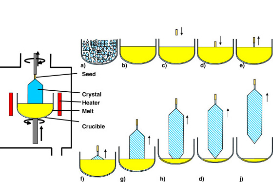
1. Czochralski Method (CZ)
The Czochralski process is a crystal growth technique used to produce large high-purity single crystals—most notably monocrystalline silicon for the electronics industry. During the process, a small seed crystal is submerged in molten material and drawn slowly up while rotating. As the crystal moves upwards, atoms in the melt are solidified onto the seed in an ordered fashion, building a cylindrical single crystal with controlled orientation and minimal defects.
The Czochralski process is capable of growing large, high-quality single crystals—typically hundreds of millimeters in diameter—under controlled temperature conditions in a clean environment. It is applied widely to materials like silicon, germanium, gallium arsenide, lithium niobate, and certain oxides. It has scalability as its primary advantage along with the ability to produce defect-free crystals, but it requires huge amounts of energy input and is not suitable for primary materials that are not congruently melting.
 [1]
[1]
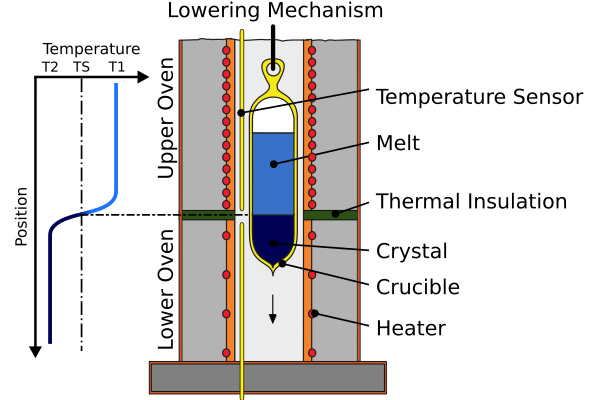
2. Bridgman–Stockbarger Technique
Bridgman–Stockbarger technique is a directional solidification which is appropriate for materials that do not get modified by being in crucibles. In the Bridgman–Stockbarger technique, the material is loaded into a crucible and melted, and thereafter carried slowly through a temperature gradient from hot to cold. Solidification begins at the cold end where a seed crystal allows the growth of a single crystal as the melt solidifies progressively.
This technique is widely applied to materials such as gallium arsenide, lead halides, cadmium telluride, and some oxides, and finds use in radiation detectors, thermoelectric devices, and infrared optics. It provides good control over crystal orientation and is employed for volatile or reactive compounds when the sealed ampoules are used. Disadvantages include the possibility of contamination from the crucible and smaller crystal sizes than those produced using the Czochralski process.
 [2]
[2]
3. Flux Growth
Flux growth is a crystal growth method particularly well suited to materials which melt incongruently or decompose prior to their melting point. The method involves the use of a flux—a solvent in effect—to dissolve the material in question at elevated temperatures. As the solution is cooled, decreasing solubility causes the crystals to precipitate and grow gradually.
This method is used often to crystallize crystals such as YAG (yttrium aluminum garnet), borates, ferrites, and complex oxides for laser technology, magnetic devices, and optical isolators applications. Its main advantages are lower growth temperatures, which minimize thermal stresses and are appropriate for sensitive compounds. Growth is slow, but residue flux removal from the products may be problematic.
4. Hydrothermal Growth
Hydrothermal growth is ideal for the growth of crystals of materials that are insoluble by other means or have very high melting points. Under the process, raw materials are dissolved in superheated water in a sealed high-pressure autoclave. A temperature gradient inside the vessel leads to the dissolution of the material at the warmer end and the gradual crystallization on a seed at the cooler end.
Primarily used for the growth of quartz, zinc oxide, lithium niobate, and barium titanate, this technique supports electronics, optics, and piezoelectric device development. It gives high-quality crystal with a significant purity but at the cost of very expensive high-pressure apparatus, long time consumptions, and heavy safety measures.
5. Physical Vapor Transport (PVT)
Physical Vapor Transport (PVT) is a sublimation-induced crystal growth process suitable for those materials which transform from solid to vapor directly without melting. In the PVT, the source material is sublimed in vacuum or inert atmosphere through heating till the vapor is deposited on a cold seed crystal to obtain a single crystal.
PVT is commonly used to grow silicon carbide (SiC), aluminum nitride (AlN), and other organic crystals, which find applications in high-power devices, UV LEDs, and advanced optics. The technique allows high-purity crystal growth with little chance of contamination, but at the expense of slow growth and precise thermal control.
6. Zone Melting
Zone melting is primarily used for material purification but can also be used for directional crystal growth. In this process, a thin zone of solid rod is melted and gradually moved along the rod. While moving along the molten zone, impurities are brought to the concentration in the melt and eliminated, leaving more ordered, purer crystal structure behind.
It is widely applied on substrates like silicon, germanium, and gallium arsenide for semiconductors and solar cells. It may have excellent impurity control and post-growth refinement, but it's generally limited to rod-shaped crystals and not applicable for mass production of wafers.
7. Vapor Phase Epitaxy (VPE) and Molecular Beam Epitaxy (MBE)
Epitaxial processes, while not used in the growth of bulk crystals, are required for thin single-crystal film growth on substrates. Reactive gases deposit material layer by layer in Vapor Phase Epitaxy (VPE), while Molecular Beam Epitaxy (MBE) is a process with atomic beams condensing on a hot substrate in the ultra-high vacuum environment.
These methods are generally used for the growth of such materials as gallium nitride (GaN), gallium arsenide (GaAs), and indium phosphide (InP) for applications in LEDs, lasers, and high-frequency transistors. They allow precise atomic-level control and purity, but only at thin films and probably costly and time-consuming procedures.
Summary Table
|
Technique |
Materials |
Applications |
Advantages |
Limitations |
|
Czochralski (CZ) |
Silicon, GaAs, lithium niobate |
Semiconductors, solar cells, optics |
Large crystals, high purity |
High energy use, not for all materials |
|
Bridgman–Stockbarger |
GaAs, CdTe, halides |
IR optics, detectors, thermoelectrics |
Good orientation control |
Crucible contamination, size limits |
|
Flux Growth |
YAG, borates, complex oxides |
Lasers, magnets |
Low temp, good for fragile compounds |
Slow growth, flux removal issues |
|
Hydrothermal Growth |
Quartz, ZnO, ferroelectrics |
Electronics, optics, sensors |
High purity, high melting point |
Long growth times, costly equipment |
|
Physical Vapor Transport (PVT) |
SiC, AlN |
Power electronics, UV LEDs |
High purity, suitable for tough materials |
Slow rates, thermal control needed |
|
Zone Melting |
Silicon, germanium |
Semiconductor purification |
Effective impurity removal |
Limited shapes, rod only |
|
Vapor Phase Epitaxy (VPE) / Molecular Beam Epitaxy (MBE) |
GaN, GaAs, InP |
LEDs, lasers, transistors |
Atomic-level control, high quality |
Thin films only, costly |
For more information, please check Stanford Electronics.
Conclusion
Single crystal growth is a pillar of modern materials engineering. As the demand for high-performance electronics, quantum computing, and renewable energy continues to rise, the importance to learn and enhance crystal growth techniques also rises.
Reference:
[1] J. Friedrich, Methods for Bulk Growth of Inorganic Crystals: Crystal Growth, Reference Module in Materials Science and Materials Engineering, Elsevier, 2016, ISBN 9780128035818.
[2] Bridgman–Stockbarger method. (2025, July 7). In Wikipedia. https://en.wikipedia.org/wiki/Bridgman%E2%80%93Stockbarger_method


 Powder for Li-ion Battery Cathodes")
