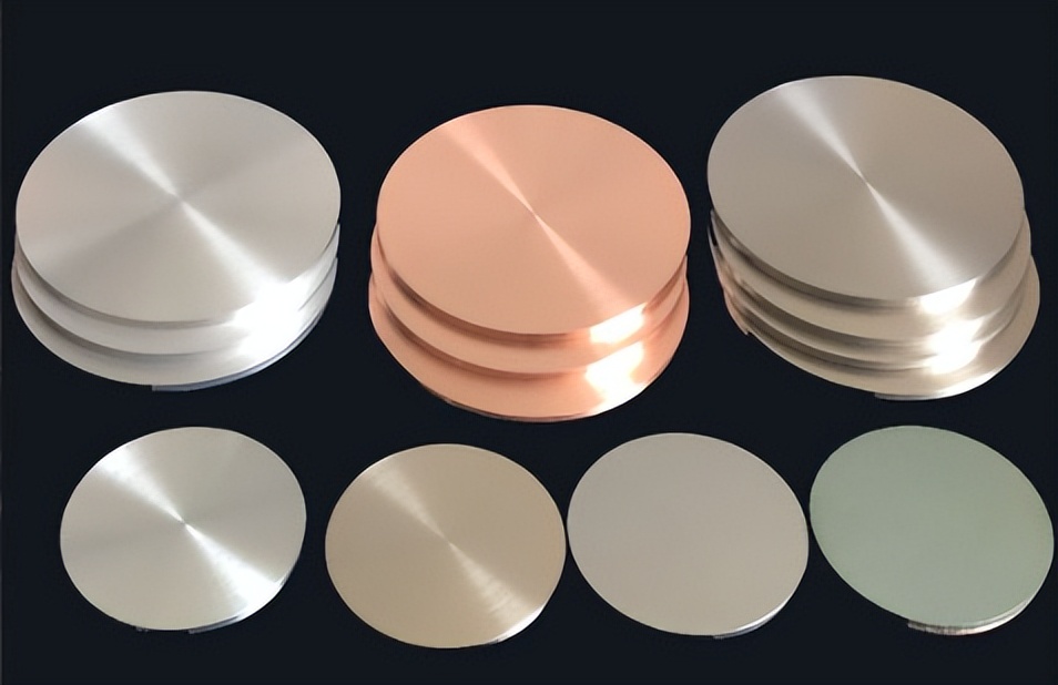
A Short Introduction to Oxide Sputtering Targets
Oxide sputtering targets are essential materials in the technology of thin-film deposition, especially in the manufacture of electronic, optical, and energy devices. These compounds—are generally ceramic in nature—they facilitate the fabrication of complex oxide films that possess favorable electrical, optical, and structural properties. Their applications span from transparent conductive coatings, dielectric coatings, barrier coatings, to functional oxides used in displays, semiconductors, solar cells, and sensors.
In this article, we will discuss why oxide sputtering targets are required and what are they primarily divided into.

What Are Oxide Sputtering Targets?
Oxide sputtering targets are solid-state sources of metal oxides that are used in physical vapor deposition (PVD) machines—namely, in sputtering processes. When bombarded with a high-energy plasma, atoms from the oxide target are ejected and deposited onto a substrate to form a thin film. The chemical composition of the target determines the physical and chemical properties of the resultant film, and oxide targets therefore play a central role in achieving the desired device characteristics.
Why Utilize Oxide Targets?
Oxide materials offer specific benefits over metals and other materials:
•Optical Transparency: Many oxides are optically transparent in the visible spectrum, making them suitable for applications like touchscreens, OLEDs, and building glass.
•Electrical Conductivity or Insulation: Certain oxides (e.g., ITO) have high conductivity while others (e.g., SiO2) have high insulation characteristics.
•Chemical and Thermal Stability: Oxide films are generally heat-, moisture-, and chemically-resistant and can be used in harsh environments.
•Stoichiometric Control: Pre-formed oxide targets or reactive sputtering enable accurate control of oxygen levels in the film, which influences functionality and longevity.
Popular Types of Oxide Sputtering Targets
1. Transparent Conductive Oxides (TCOs)
•Indium Tin Oxide (ITO): The most well-known TCO, ITO, maintains high electrical conductivity while being highly transparent. It is employed in flat panel displays, touch panels, and photovoltaic devices. Its function is regulated by the indium-tin content, deposition situation, and post-annealing treatments.
•Aluminum-Doped Zinc Oxide (AZO): AZO is an inexpensive, eco-friendly substitute for ITO. It is capable of decent transparency and conductivity, particularly for large-area display panels and thin-film solar cells.
•Gallium-Doped Zinc Oxide (GZO): GZO provides higher thermal stability and is increasingly being applied to flexible OLED displays where durability is emphasized.
•Fluorine-Doped Tin Oxide (FTO): FTO has widespread application in low-cost devices like architectural glass and certain solar cells. It is less conductive than ITO but more chemically stable.
Further reading: Comparing Transparent Conducting Oxides: ITO, AZO, and FTO
2. Dielectric and Insulating Oxides
•Silicon Dioxide (SiO2): SiO2 is a key insulating compound used in microelectronics. It provides electrical insulation, acts as a barrier layer, and protects against environmental stress.
•Aluminum Oxide (Al2O3): Being hard and thermally stable, Al2O3 acts as a passivation and dielectric layer in electronic devices and optical coatings.
•Hafnium Oxide (HfO2): HfO2 is used in high-k dielectric technology, which is mostly used in gate arrays of next-generation CMOS transistors. It allows better leakage current control and high capacitance.
•Zirconium Oxide (ZrO2): It is used in sensors, thermal barrier coatings, and a high-k dielectric material in memory devices due to its chemical stability and high melting point.
3. Functional Oxides for Electronics and Sensors
•Titanium Oxide (TiO2): Used in photocatalytic coatings, optical filters, and as an anti-reflective coating. Optical properties of TiO2 can be controlled through doping and deposition parameters.
•Niobium Oxide (Nb2O5): Used in electrochromic and optical devices, niobium oxide offers controllable coloration behavior and refractive indices.
•Bismuth Oxide (Bi2O3): Used in sensors and certain display technologies, this oxide offers unique dielectric and optical properties.
Applications of Oxide Sputtering Targets
•Displays: Oxide sputtering targets are used in LCD, OLED, and microLED displays to produce transparent electrodes and pixel control layers to enable clear images and precise display performance.
•Semiconductors: Oxide targets are used as dielectric layers, gate insulators, and barrier films in the semiconductor industry, enabling device reliability and miniaturization.
•Photovoltaics: The targets are used as front electrodes and buffer layers in thin-film solar cells, which enhance light absorption and electric efficiency.
•Smart Windows: Oxide materials are utilized in electrochromic and thermochromic smart window systems to regulate indoor temperature and reduce energy consumption.
•Sensors: Oxide sputtering targets are applied in sensing mechanisms in gas sensors, biosensors, and photodetectors to enhance sensitivity, stability, and response time.
Conclusion
Oxide sputtering targets will be essential in offering the next generation of electronics, energy, and smart surfaces. With the ability to offer transparent, conducting, insulating, or functional films—these materials benchmark the performance and life span of thin-film technology. For more information, please visit Stanford Electronics.


