
Applications and Performance Demands of Metallic Sputtering Targets
Many people have probably utilized devices or products that utilize metallic sputtering targets without even realizing it. Anyone who has had any kind of interaction with modern electronics, solar cells, or flat panel displays has had an indirect experience with these very essential materials. As a premier provider of metallic sputtering targets, the question Stanford Electronics gets asked a lot is: "What exactly are metallic sputtering targets?", and "Which kind do I need to select for my requirements?"
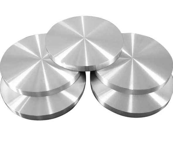
Stanford Electronics provides customized metallic sputtering targets made from high purity metals and alloys, carefully designed according to specific requirements of purity level, thickness, and uniformity. These are required in a wide range of physical vapor deposition applications in semiconductors, electronics, energy, and tooling applications.
Semiconductor Integrated Circuits
Sputtering targets used in the semiconductor industry are an important component of conductive, barrier, or adhesion films found within integrated circuits (ICs), particularly when made up of ultra-high-purity materials such as tantalum, titanium, or copper. The prime requirements are:
- High purity of the material to eliminate defects
- Nanometer-level thickness control for precise layers
- Uniform thin films for the stringent requirements of semiconductor chip manufacturing
Flat Panel Displays
Sputtering targets are critical components in the fabrication of LCD displays, OLED displays, and laptop displays. They are used for the deposition of transparent electrodes and metals such as Indium Tin Oxide (ITO), Aluminum (Al), Copper (Cu), and Molybdenum (Mo). Some of the performance specifications are:
- Large Area Film Uniformity for uniform display quality
- Excellent optical and electrical qualities
- Material purity required in mass production.
Thin-Film Solar Cells
In the field of renewable energy, metallic targets are used in depositing electrode and back contact layers in thin-film solar cells in CIGS (copper indium gallium selenide), CdTe (cadmium telluride), and other cells. These are molybdenum (Mo), copper (Cu), indium (In), and ITO. These must offer:
- Coatings with high stability and homogeneity
- Strong substrate adherence
- Stain resistance is improved
Data Storage Devices
Sputtering targets used for magnetic and reflecting layers on hard disk drives, optical storage media, etc. The targets are made from Co and Cr alloys.
The requirements for applications:
- Mechanical advantages due to low magnetic anisotropy, such as
- Uniform deposition for reliable read/write operations
- Structural Stability for Long-Term Stability
Coatings for Tools, Coating Surfaces
In tooling technology, sputtering targets are made of metallic materials and are used in hardened coatings of cutting tools, molds, and wear-resistant coatings. Some commonly used materials are Titanium (Ti), Chromium (Cr), and alloys of either TiAl or CrAl. Coating Requirements are:
- High hardness to provide wear resistance
- Stability to high temperatures and chemically reactive environments
- High base material adhesion
Electronic Components
Sputtering targets are used in electronic passive components like chip resistors, chip capacitors, and connectors. The most common alloys are nickel (Ni) and tin (Sn). The specifications for sputtering targets are as follows:
• Compatibility with miniaturized components
• Performance in changing electric conditions
• Low temperature coefficient of resistance (TCR) for stable performance
Other Applications
In addition to high technology industries, the use of sputtering targets is also seen in the following fields: decorative and functional coatings, architectural glass, energy-efficient windows, and films. Other common target materials include gold (Au), titanium (Ti), and chromium (Cr). The requirements for the target materials are:
- Aesthetic quality and uniform appearance
- Oxidation and corrosion resistance
- Cost-efficiency in mass production
Table 1 Metallic Sputtering Targets, Applications, and Requirements
|
Application |
Common Materials |
Key Performance Demands |
|
Semiconductor Integrated Circuits |
Tantalum (Ta), Titanium (Ti), Copper (Cu) |
Ultra-high purity, nanometer-level thickness, uniform films |
|
Flat Panel Displays |
ITO, Aluminum (Al), Copper (Cu), Molybdenum (Mo) |
Large-area uniformity, optical/electrical performance, high purity |
|
Thin-Film Solar Cells |
Molybdenum (Mo), Copper (Cu), Indium (In), ITO |
Stable coatings, strong adhesion, cost-effective deposition |
|
Data Storage Devices |
Cobalt (Co) alloys, Chromium (Cr) |
High magnetic performance, uniform deposition, structural stability |
|
Tool Coatings |
Titanium (Ti), Chromium (Cr), TiAl, CrAl alloys |
Hardness, thermal/chemical stability, excellent adhesion |
|
Electronic Components |
Nickel (Ni) alloys, Tin (Sn) alloys |
Miniaturization, electrical stability, low TCR |
|
Other Applications |
Gold (Au), Chromium (Cr), Titanium (Ti) |
Aesthetic quality, oxidation resistance, economical processing |
Conclusion
Metal sputtering materials are basic materials in a variety of industries, including microchip production, flat panel displays, solar cells, cutting tool coatings, and decorative coatings, each having its specific performance requirements but including the need for high purity, precise deposition, good adhesion, and good thin-film properties.
However, as the new technologies become more compact, faster, and more complicated, the demand for high-quality sputtering targets is of utmost importance. If a manufacturer chooses to acquire its targets from a reputable source, such as the Stanford Electronics, it would be able to benefit from high-quality sputtering targets.


 Powder for Li-ion Battery Cathodes")
