
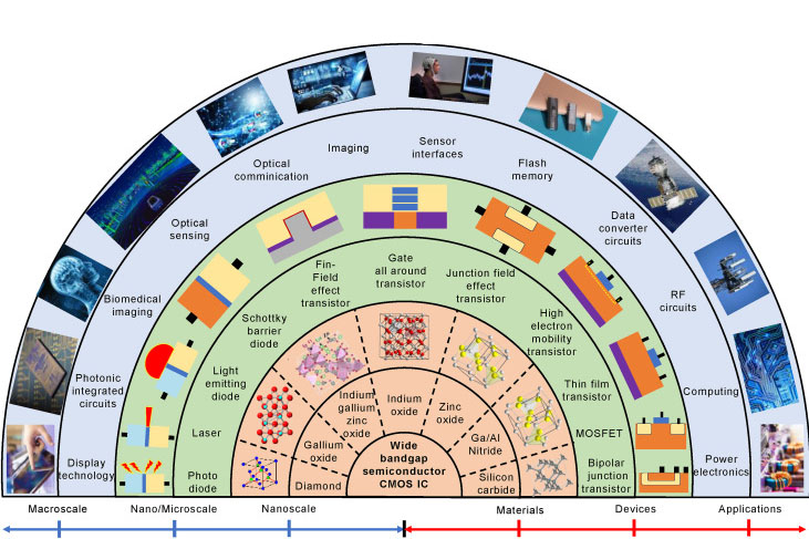
Everything You Want to Know about Wide-Bandgap Semiconductors
Wide-bandgap semiconductors are revolutionizing the world of electronics by supporting voltage, temperature, and switching rates that were previously impossible for silicon semiconductors to handle. They have numerous usages in electric vehicles, renewable energy, 5G networks, etc. We will examine the definition of a "wide band gap" semiconductor, the reasons for their popularity, and their current use.
[1]
What Constitutes A Wide Band Gap?
In semiconductor physics, band gap can be referred to as the difference in energy values of the valence band and the conduction band of any material. The band gap normally determines how easily electrons can flow or conduct through a material. When a semiconductor has a small band gap, very little energy is needed to translate electrons to the conduction band.
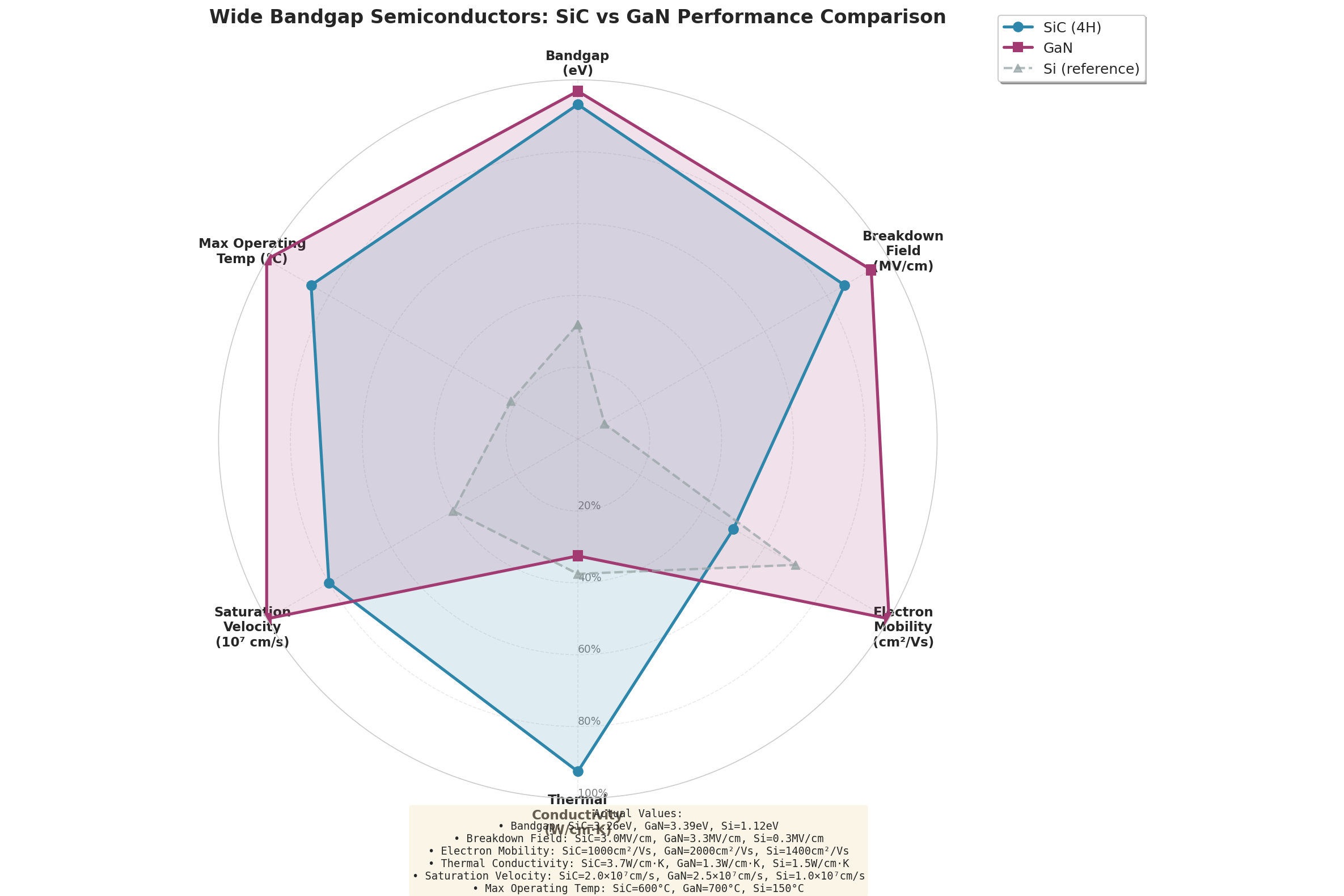
A wide bandgap semiconductor is considered to be a semiconductor that has a band gap much wider than that of silicon semiconductors. Silicon is considered the most commonly used semiconductor material, and it has a band gap of around 1.12 eV at room temperature. Wide bandgap semiconductors normally tend to have a band gap over 2.0 eV.
To illustrate, the band gaps for silicon carbide (SiC) vary between 2.3 and 3.3 eV, depending upon the polytype, while the band gap for Gallium Nitride (GaN) stands at approximately 3.4 eV. Such wide band gaps completely alter the operating characteristics of the devices when subjected to electrical stress, elevated temperatures, and high frequencies, paving the way for use cases that are not feasible in regular semiconductors.
Why Are Wide-Bandgap Semiconductors Better?
"Better" wide bandgap semiconductors are deemed such not because they will displace silicon in all situations, but where today's silicon-based devices are inefficient or unreliable.
One of the most significant benefits is that the electrical breakdown strength increases. The wide-bandgap materials can resist much stronger electric fields, making it possible to use higher voltages and still achieve a compact design. The effect is a reduced and lightweight power electronics system designed with fewer components.
Another important aspect is the ability to operate at higher temperatures. Silicon devices were not designed to handle temperatures above 150°C, but wide-bandgap devices can handle temperatures above 300°C. This makes the devices more suitable for applications in the automotive and aeronautical fields, which require devices to withstand high temperatures.
Wide band gap semiconductors have lower switching losses and higher switching speeds. The material characteristics of wide band gap semiconductors enable easier movement of electrons, thus switching can be done effortlessly and with less energy being converted to heat. This makes them suitable for high frequency power conversions, where even small improvements in efficiency translate to substantial energy savings.
Furthermore, there are wide band gap materials which show high thermal conductivity and radiation tolerance, which make them useful for applications like space, nuclear power, and high-power RF. Combining these factors, it becomes possible for researchers and system designers to create more efficient, smaller, and longer-lasting devices compared to what can be developed from regular semiconductor materials.
Which Semiconductor Materials have A Large Band Gap?
There are a few semiconductor materials that belong to wide-bandgap materials and each material has its own merits and applications.
Silicon Carbide (SiC) is considered to be the most mature semiconductor material in the wide bandgap family. It has band gaps ranging from 2.3eV to 3.3eV, depending upon the crystal structure. It has been found to possess high breakdown voltage, high thermal conductivity, and stability against chemicals.
Gallium Nitride (GaN) has a large band gap of approximately 3.4 eV; hence, GaN is preferred in high-speed and high-frequency designs. GaN technology enables a high-speed transition and low losses, making GaN an ideal choice for RF amplifiers, high-speed chargers, and high-end power supplies.
Ga₂O₃ is a rising ultra-wide bandgap semiconductor that possesses a band gap value of around 4.8-4.9 eV. Ga₂O₃ is also characterized by a very high breakdown field that makes it useful as future high voltage power devices; despite that, its processing is an area of current research studies.
Diamond, having an approximated band gap of 5.5 eV, is at the end of the wide band gap semiconductors. Although its extraordinary properties, both electrical and thermal, are widely recognized, expense and the difficulty of diamond production so far have restricted diamond application only to some niche uses like radiation detectors and electronics.
What Are the Uses of Wide-Bandgap Semiconductors?
Wide bandgap materials have already started changing some sectors, mostly those that require efficiency, power density, and reliability.
In power electronics, SiC and GaN semiconductors are making possible smaller and more efficient power converters, inverters, and motor drives. Both are utilized extensively in electric vehicles because they increase range through reduced losses in traction inverters and DC onboard chargers. Even charging infrastructure experiences improved switching speed and efficiency with smaller and high-power fast charging stations being built.
In the field of renewable energy, wide bandgap semiconductors serve as important constituents of solar inverters as well as wind energy converters. The fact that these semiconductors can efficiently withstand higher voltages as well as temperatures increases system reliability by optimizing the available useful power output.
The other important application field is telecommunications and RF electronics. GaN technology is applied in 5G base stations, satellite communications, and radar applications because of the materials' high power density and good high-frequency characteristics. Such qualities facilitate the creation of signals with higher intensity, higher bandwidth, and smaller RF modules.
Other areas where wide band gap semiconductor materials play a vital role include industrial applications, as well as the aero industry. The technology used in high temperature sensors, power modules in aero planes, and space-level electronics requires resistant properties such as that of SiC and GaN.
Lastly, in consumer electronics, GaN has also attracted considerable attention for its usage in the development of fast chargers or power adapters that consume minimal space. This is due to the fact that GaN chips function at higher frequencies with negligible loss.
Conclusion
Wide-band gap semiconductors mark a paradigm shift in electronics design and optimization. With wider band gaps, greater breakdown voltages, superior thermolelectric characteristics, and higher switching speeds, these materials and technology negate the limitations that exist in conventional semiconductor technology. Although issues exist with respect to cost, manufacturing, and material quality, continuous improvements are increasingly establishing them as viable commercial options. With industries increasingly requiring greater efficiency, power density, and reliability, wide-band gap semiconductors will increasingly define the future of electronics.
Reference:
[1] Saravanan Yuvaraja, Vishal Khandelwal, Xiao Tang, Xiaohang Li, Wide bandgap semiconductor-based integrated circuits, Chip, Volume 2, Issue 4, 2023, 100072, ISSN 2709-4723.


 Powder for Li-ion Battery Cathodes")
