
Gallium Nitride Transistors: The Future of High-Power and High-Frequency Electronics
For more than half a century, silicon has been the foundation of the electronics industry. From microprocessors to power converters, silicon transistors have enabled the modern digital world. Yet as electronic systems push toward higher power densities, faster switching speeds, and more extreme operating environments, the physical limits of silicon are becoming increasingly apparent.
Gallium nitride (GaN) transistors have emerged as one of the most promising successors. As a wide-bandgap semiconductor technology, GaN is redefining what is possible in high-power and high-frequency electronics, opening the door to smaller, faster, and more energy-efficient systems across a wide range of industries.
 [1]
[1]
The Material Advantage of Gallium Nitride
Gallium nitride belongs to a class of materials known as wide-bandgap semiconductors, characterized by a larger bandgap energy than silicon. GaN's bandgap is about 3.4 eV, nearly three times that of silicon. This fundamental property leads directly to several performance advantages. A wider bandgap allows GaN devices to withstand much higher electric fields before breakdown, enabling transistors that operate at higher voltages and deliver more power in a smaller footprint.
In addition, GaN exhibits high electron mobility and a high saturation velocity, meaning charge carriers can move quickly through the crystal lattice. This translates into extremely fast switching speeds and excellent performance at radio and microwave frequencies. GaN also has superior thermal stability compared with silicon, maintaining reliable operation at elevated junction temperatures where silicon devices would suffer from leakage, degradation, or outright failure.
Together, these intrinsic material properties form the basis of GaN's appeal for applications that demand both high power handling and high-frequency operation.
Device Architecture: The Rise of the GaN HEMT
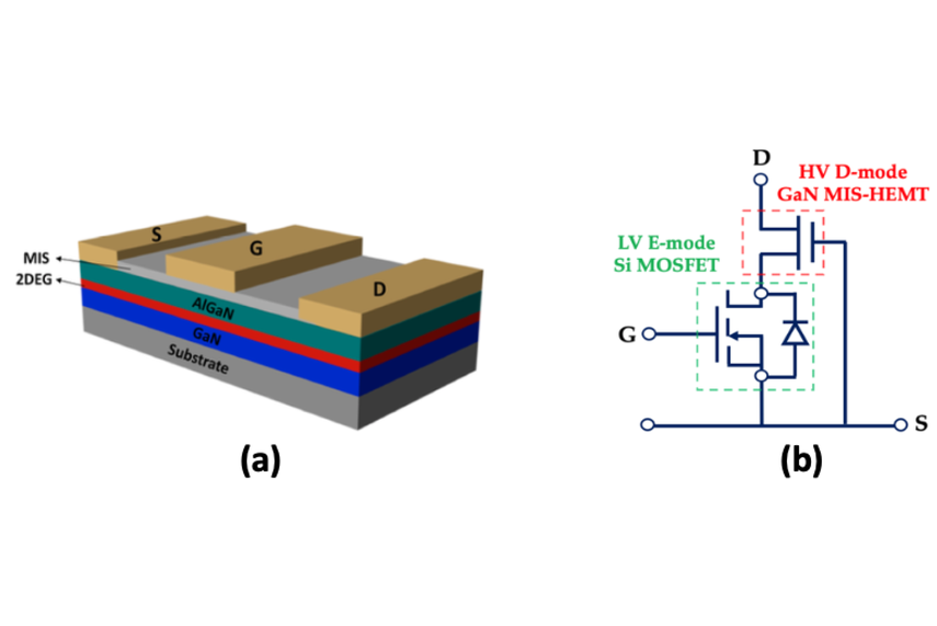
Most commercial GaN transistors today are based on the high-electron-mobility transistor (HEMT) architecture. In a GaN HEMT, a heterostructure is formed by stacking gallium nitride with aluminum gallium nitride (AlGaN). At the interface between these two materials, a two-dimensional electron gas (2DEG) forms naturally, without intentional doping. This 2DEG has exceptionally high carrier density and mobility, providing a low-resistance conduction channel that supports both high current and high switching speed.
GaN HEMTs can be fabricated in "normally-on" (depletion-mode) or "normally-off" (enhancement-mode) configurations. For power electronics, normally-off devices are preferred because they are inherently safer and more compatible with conventional gate-drive circuits. Advances in gate engineering, p-GaN gate structures, and cascode configurations have made normally-off GaN transistors widely available and reliable.
High-Power Performance: Smaller, Faster, More Efficient
One of the most compelling advantages of GaN transistors is their ability to handle high power with dramatically reduced losses. GaN devices exhibit very low on-state resistance and minimal switching losses, allowing them to operate efficiently at much higher switching frequencies than silicon MOSFETs or even silicon carbide (SiC) devices in some voltage ranges.
Higher switching frequency has a cascading impact on system design. Inductors, transformers, and capacitors can be made much smaller, reducing the overall size and weight of power converters. This is particularly valuable in applications such as fast chargers, data center power supplies, and onboard power systems for electric vehicles, where efficiency and compactness directly translate into lower energy consumption and higher power density.
In modern consumer electronics, GaN transistors have already revolutionized fast charging. Compact chargers delivering 65 W, 100 W, or even higher power levels are now possible in form factors that were unimaginable a decade ago. In industrial and automotive power systems, GaN enables higher efficiency and reduced cooling requirements, lowering operating costs and improving reliability.
High-Frequency Excellence: Enabling Next-Generation RF Systems
Beyond power conversion, GaN transistors excel in high-frequency and microwave applications. Their high breakdown field and fast carrier dynamics make them ideal for radio-frequency (RF) power amplifiers operating from hundreds of megahertz into the millimeter-wave regime.
In wireless infrastructure, GaN transistors are becoming the technology of choice for 5G and emerging 6G base stations. They provide higher output power, wider bandwidth, and better efficiency than traditional silicon LDMOS devices, enabling more compact and energy-efficient transmitters. In radar and satellite communications, GaN amplifiers offer higher power density and improved reliability under harsh environmental conditions, including high temperature, vibration, and radiation.
Defense and aerospace systems, which often require operation at high frequencies and extreme power levels, have been among the earliest adopters of GaN technology. The ability of GaN devices to maintain stable performance at elevated temperatures and high voltages makes them particularly well suited for these demanding applications.
Substrates, Manufacturing, and Integration Challenges
Despite its remarkable properties, GaN is not without challenges. Native bulk GaN substrates are expensive and limited in size, so most GaN transistors are grown epitaxially on foreign substrates such as silicon, silicon carbide, or sapphire. Each option involves trade-offs in thermal conductivity, lattice mismatch, cost, and wafer size.
GaN-on-silicon offers cost advantages and compatibility with large-diameter wafers, making it attractive for mass production in consumer and industrial markets. GaN-on-SiC provides superior thermal performance and is favored for high-power RF and defense applications, albeit at higher cost.
Device packaging and thermal management also remain critical areas of development. Because GaN transistors can operate at very high power densities, efficient heat extraction is essential to fully realize their performance potential. Advanced packaging techniques, including flip-chip mounting, integrated power modules, and wide-bandgap-compatible gate drivers, are rapidly evolving to meet these demands.
Reliability and Long-Term Stability
As GaN technology matures, reliability has become a central focus. Early concerns about gate leakage, current collapse, and long-term degradation have been addressed through improved epitaxial growth, surface passivation, and device design. Today's commercial GaN transistors meet stringent qualification standards for automotive, industrial, and aerospace use.
Nevertheless, understanding failure mechanisms under high electric fields, high temperature, and fast switching remains an active area of research. Continued progress in reliability testing and modeling will be essential as GaN devices move into safety-critical systems such as electric vehicles and aircraft power electronics.
A Defining Technology for the Next Electronics Era
Gallium nitride transistors represent a fundamental shift in how engineers approach high-power and high-frequency electronics. By combining wide-bandgap material properties with innovative device architectures, GaN offers performance levels that silicon simply cannot match. The result is a new generation of electronic systems that are smaller, faster, cooler, and more energy-efficient.
From fast chargers and data centers to 5G networks, electric vehicles, and advanced radar systems, GaN transistors are already reshaping multiple industries. As manufacturing scales, costs continue to fall, and reliability further improves, GaN is poised to become a cornerstone technology of modern power and RF electronics. In many respects, it is not merely the future of high-power and high-frequency electronics—it is rapidly becoming the present. For more information, please check Stanford Electronics.
Reference:
[1] Elangovan, Surya & Cheng, Stone & Yi-Chang, Edward. (2020). Reliability Characterization of Gallium Nitride MIS-HEMT Based Cascode Devices for Power Electronic Applications. Energies. 13. 10.3390/en13102628.


 Powder for Li-ion Battery Cathodes")
