
Essential Electronic Materials: Part 4 - Gallium Compounds
Gallium-based compounds, including gallium oxide (Ga₂O₃), gallium arsenide (GaAs), and gallium nitride (GaN), have gained significant attention in the fields of electronics and semiconductors due to their exceptional physical and chemical properties. These materials exhibit a wide range of electrical, optical, and thermal characteristics, making them indispensable for advanced technologies.
- Gallium oxide (Ga₂O₃): Known for its ultra-wide bandgap and high breakdown electric field, Ga₂O₃ is emerging as a promising material for high-power electronics, ultraviolet (UV) photodetectors, and other optoelectronic applications.
- Gallium arsenide (GaAs): A direct bandgap semiconductor with superior electron mobility and high-frequency performance, GaAs has long been a cornerstone in optoelectronic devices such as lasers, LEDs, and photovoltaic cells.
- Gallium nitride (GaN): With its wide bandgap, high thermal conductivity, and excellent efficiency, GaN has revolutionized power electronics and high-frequency communication systems.
1. Gallium Oxide (Ga₂O₃)
Gallium oxide, with the chemical formula Ga₂O₃, is an inorganic compound and a wide-bandgap semiconductor (Eg = 4.9 eV). Its conductivity and luminescence properties have attracted significant attention. Ga₂O₃ is a transparent oxide semiconductor material with broad application prospects in optoelectronic devices, such as insulating layers in Ga-based semiconductors, UV filters, and O₂ chemical detectors.
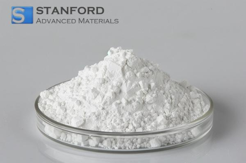
Fig. 1 Gallium Oxide Powder
Crystal Structure of Gallium Oxide
Ga₂O₃ exists in five primary crystal structures: β-Ga₂O₃, α-Ga₂O₃, γ-Ga₂O₃, δ-Ga₂O₃, and ε-Ga₂O₃.
- β-Ga₂O₃: Monoclinic crystal system with space group P21. It exhibits high electron mobility, a wide direct energy gap, and good thermal stability. Applications include high-power semiconductor devices and deep-ultraviolet optoelectronic devices.
- α-Ga₂O₃: Tetragonal crystal system with space group C4V. It is an excellent optical material with high light transmittance and corrosion resistance, used in optoelectronics and communications.
- γ-Ga₂O₃: Cubic crystal system with space group Ia3. It has high optical transmittance, low defect density, and high magnetic permeability, making it suitable for magneto-optical and UV detector devices.
- δ-Ga₂O₃: Orthorhombic crystal system with space group Pnma. It has a high bandgap, excellent photovoltaic properties, and good physicochemical stability.
- ε-Ga₂O₃: Trigonal crystal system with space group R3c. It exhibits high carrier mobility, thermal stability, and UV response properties, making it suitable for UV detectors and power electronics.
Table 1: Comparison of Different Ga₂O₃ Structures
|
|
β-Ga2O3 |
α-Ga2O3 |
γ-Ga2O3 |
δ-Ga2O3 |
ε-Ga2O3 |
|
Crystal Structure |
Monoclinic Crystal System |
Tetragonal Crystal System |
Cubic Crystal System |
Orthogonal Crystal System |
Tripartite Crystal System |
|
Space Group |
P21 |
C4V |
Ia3 |
Pnma |
R3c |
|
Cell Parameters |
a=12.203 b=5.671 c=6.524 β=105.76 |
a=12.22 c=5.86 |
a=13.54 |
a=7.794 b=5.580 c=5.395 |
a=7.794 b=5.580 c=5.395 |
|
Properties |
High electron mobility |
High light transmittance |
High optical transmittance |
High bandgap |
High carrier mobility |
|
Wide direct energy gap |
Good corrosion resistance |
Low defect density |
Excellent optoelectronic properties |
High thermal stability of the material |
|
|
Good thermal stability |
- |
High magnetic permeability |
Good physicochemical stability |
Good UV response characteristics |
|
|
Applications |
High-power semiconductor devices and deep-ultraviolet optoelectronic devices |
Optoelectronics and optoelectronic communications |
Potential use in magneto-optical devices and UV detector devices |
- |
Ultraviolet detectors, power electronics |
Physical and Chemical Properties of Ga₂O₃
Gallium oxide (Ga₂O₃) exhibits distinct chemical, thermal, and electronic characteristics that make it valuable in advanced technologies. Chemically, it reacts with fluorine gas to form gallium fluoride (GaF₃) and dissolves in dilute acids, while remaining insoluble in concentrated acids or strong bases unless fused with sodium or potassium hydroxide. From a thermal and materials perspective, Ga₂O₃ readily reacts with metal oxides to form gallates, which are widely used in lasers, phosphors, and other luminescent materials. In addition, its ultra-wide bandgap, high breakdown electric field strength, and low on-resistance give Ga₂O₃ exceptional semiconductor performance for high-power and high-temperature electronic applications.
Preparation of Ga₂O₃
Gallium oxide (Ga₂O₃) can be produced through several established methods depending on purity and application requirements. The direct reduction method involves reacting nitrogen with metallic gallium to form gallium nitride, which is subsequently oxidized to obtain Ga₂O₃. Chemical vapor deposition (CVD) relies on gaseous precursors such as GaCl₃ to deposit high-purity gallium oxide, making it suitable for electronic and optical applications. The acid method is a more traditional chemical route that includes oxidation, neutralization, filtration, washing, drying, roasting, grinding, and final packaging to produce Ga₂O₃ powders for industrial use.
Applications of Ga₂O₃
1. Power Electronics: Ga₂O₃'s high breakdown electric field and low on-resistance make it suitable for high-voltage and high-power devices, such as motor drives and smart grid systems.
2. Optoelectronic Devices: Used in UV detectors and deep-UV LEDs for environmental monitoring, sterilization, and semiconductor manufacturing.
3. Sensors: Ga₂O₃ is used in humidity, temperature, gas, and pressure sensors due to its chemical and electrical properties.
4. Other Applications: Includes flexible displays, battery materials, and radio-frequency applications like radar systems and satellite communications.
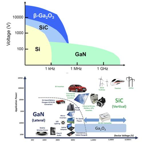
Fig. 2 Comparison of Applications of SiC, GaN and Ga2O3
2. Gallium Arsenide (GaAs)
Gallium arsenide, with the chemical formula GaAs, is a black-gray solid with a melting point of 1,238°C. It is a III-V compound semiconductor with a sphalerite-type lattice structure and a bandgap of 1.4 eV.
Crystal Structure of GaAs
GaAs has a face-centered cubic (FCC) structure, with Ga atoms at the lattice vertices and As atoms at the face centers. The lattice constant is a = 5.6535 Å.
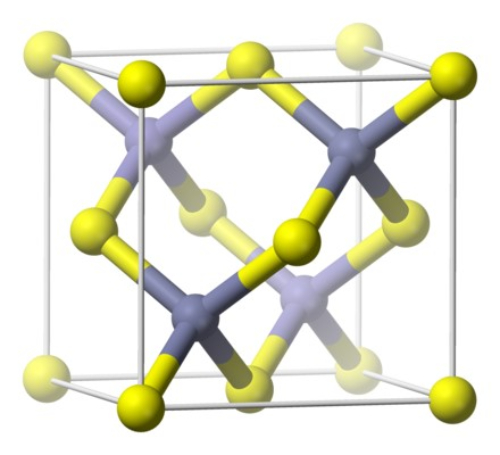
Fig. 3 Crystal Structure of Gallium Arsenide
Physical and Chemical Properties of GaAs
Table 2: Physical Properties of GaAs
|
Density |
5.31g/cm3 |
|
Melting Point |
1238℃ |
|
Refraction Index |
3.57 |
|
Relative Permittivity |
13.18 |
|
Electron Affinity Energy |
4.07eV |
|
Lattice Energy |
5.65×10⁻¹⁰m |
|
Band Gap |
1.424e(300K) |
|
Electron Mobility |
8500cm2/(V·s)(300K) |
|
Appearance |
Black-Grey Solid |
Preparation of GaAs
Gallium arsenide (GaAs) can be manufactured using several crystal growth and deposition techniques tailored to different performance requirements. Vertical Gradient Solidification (VGF) is widely used to produce high-quality GaAs single crystals with excellent structural uniformity. The Liquid Encapsulation Czochralski (LEC) method is commonly applied to grow semi-insulating GaAs crystals by suppressing arsenic evaporation during pulling. The Horizontal Bridgman (HB) method enables the production of GaAs crystals with low dislocation density, while Chemical Vapor Deposition (CVD) is employed to deposit high-purity GaAs thin films for electronic and optoelectronic applications.
Applications of GaAs
1. Microwave Field: Used in high-frequency devices like HEMTs and LEMTs for wireless communications and radar systems.
2. Optoelectronics: GaAs is used in lasers, LEDs, and solar cells due to its direct bandgap.
3. Communication: Used in fiber optic communication devices like optical receivers and amplifiers.
4. Solar Cells: GaAs solar cells offer high efficiency and stability.
5. Microelectronics: Used in high-speed circuits, flash memory, and power transistors.
3. Gallium Nitride (GaN)
Gallium nitride, with the chemical formula GaN, is a third-generation semiconductor material known for its wide bandgap, high thermal conductivity, and chemical stability.
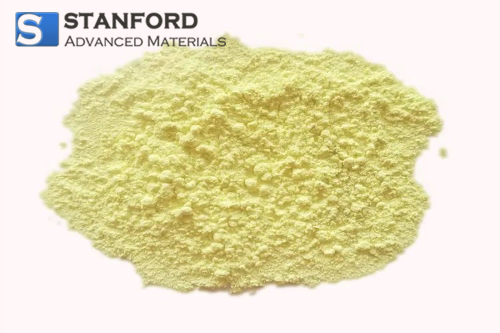
Fig. 4 Gallium Nitride Powder
Crystal Structure of GaN
GaN has a hexagonal wurtzite structure, with each Ga atom bonded to four N atoms. The lattice constant is a = 3.189 Å and c = 5.185 Å.
Properties of GaN
Gallium nitride (GaN) is a wide-bandgap semiconductor with an energy gap of about 3.4 eV, giving it high transparency across the visible spectrum. It exhibits excellent mechanical strength, with high hardness and a strong modulus of elasticity, along with favorable thermal properties such as high thermal conductivity and low thermal expansion. Optically, GaN shows low absorption in the visible region, making it suitable for optoelectronic devices. Its strong chemical stability provides resistance to acids, alkalis, and oxidation. In addition, GaN offers outstanding electronic performance, including high electron mobility and a high saturation drift velocity, which supports high-power and high-frequency applications.
Preparation of GaN
GaN is typically grown using MOCVD, MBE, or HVPE techniques. The reaction involves the decomposition of TMGa and NH₃ at high temperatures.
Applications of GaN
1. Power Electronics: GaN is used in high-power and high-frequency devices like HEMTs and MOSFETs.
2. Optoelectronics: GaN is the material of choice for blue and green LEDs, lasers, and UV detectors.
3. Sensors: GaN is used in pressure, temperature, gas, and optical sensors due to its stability and sensitivity.
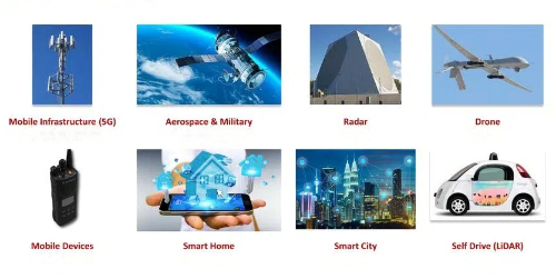
Fig. 5 Applications of Gallium Nitride
Conclusion
Gallium-based compounds, including Ga₂O₃, GaAs, and GaN, are at the forefront of modern semiconductor technology. Each material offers unique advantages:
- Ga₂O₃: High-power and high-voltage applications.
- GaAs: High-speed and optoelectronic devices.
- GaN: Power electronics and high-frequency communication systems.
Stanford Electronics is a leading provider of high-quality gallium materials, supporting these critical applications with reliable material solutions.
Further Reading:
Essential Electronic Materials: Part 1 - Silicon


 Powder for Li-ion Battery Cathodes")
