
Essential Electronic Materials: Germanium Fabrication and Properties
Introduction
Germanium (Ge), a semiconductor material with a diamond-like crystal structure, has unique physical and electrical properties that make it indispensable in certain high-tech applications.
With an atomic number of 32 and a density of 5.323 g/cm³, it has a small bandgap of 0.66 eV, granting it superior electrical conductivity at low temperatures. While silicon dominates the semiconductor industry, germanium plays a critical role in high-frequency electronics, solar cells, and infrared optoelectronics, including fiber-optic communication and infrared detectors. Its ability to integrate with silicon also enhances its relevance in advanced integrated circuit technologies.
However, challenges such as lower thermal conductivity, high production costs, and difficulties in scaling its crystal growth hinder its broader adoption.
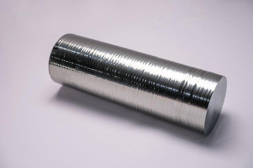
Fig. 1 Germanium Single Crystal
Basic Properties of Germanium
Germanium, a member of Group IVA of the periodic table, shares similarities with tin and lead but stands out due to its advanced semiconductor characteristics. It exists naturally with five stable isotopes. Chemically stable at room temperature, germanium reacts with oxygen above 700°C to form GeO2 and with hydrogen above 1,000°C. Its brittleness (Mohs hardness of 6.0) limits its mechanical applications, but its optical and electronic properties make it invaluable in specific domains.
With a melting point of 937.4°C and a boiling point of 2,833°C, germanium has low thermal conductivity (60 W/m·K) compared to metallic materials, making it less effective for high-temperature applications. However, its exceptional infrared sensitivity (particularly at a wavelength of 1.55 μm) ensures its widespread use in fiber-optic communications and infrared detectors. Additionally, its atomic volume (13.6 cm³/mol), density (5.35 g/cm³), and high conductivity at room temperature (1.6 × 10³ S/m) highlight its unique suitability for low-temperature and high-frequency applications.
Table 1 Physical Properties of Germanium
|
Property |
Value |
|
Appearance |
Dark blue, crystalline, silvery-white, brittle metal |
|
Valence |
+2, +4 |
|
First Ionization Energy |
7.899 eV |
|
Solubility |
Insoluble in water |
|
Atomic Volume |
13.6 cm³/mol |
|
Relative Atomic Mass |
72.64 |
|
Mohs Hardness |
6 |
|
Rate of Sound Propagation |
5400 m/s |
|
Density |
5.35 g/cm³ |
|
Melting Point |
937°C |
|
Boiling Point |
2830°C |
|
Heat and Light Coefficient |
dn/dT ≈ 0.0004/K (25°C–150°C) |
For more information, please check Stanford Electronics.
Fabrication Processes for Germanium
Two primary methods dominate the production of germanium single crystals: the Czochralski method and the Vertical Gradient Freezing (VGF) method. These techniques are vital for obtaining high-purity single crystals essential for semiconductor and optoelectronic devices.
Czochralski Method
The Czochralski method, widely used in the semiconductor industry, produces large-sized, high-purity single crystals with low defect densities. This process involves pulling a germanium crystal seed from a melt while controlling parameters like temperature and pulling speed to ensure uniform growth.
Steps in the Czochralski Method:
- Preparation of Raw Materials:
High-purity germanium (99.999% or higher) or germanium alloys serve as the feedstock. The material is melted in a high-temperature furnace, often using quartz or platinum crucibles to avoid chemical reactions with the molten germanium. - Melting:
The temperature is maintained slightly above the melting point of germanium (937.4°C), typically between 1,050°C and 1,150°C, to ensure a homogeneous liquid state. Impurities and bubbles are minimized during this stage. - Seeding and Crystal Growth:
A high-quality germanium single-crystal wafer, often oriented along the <100> or <111> plane, is used as the seed crystal. The seed is immersed in the molten germanium, and as it is slowly pulled vertically (0.5–2 mm/min), germanium atoms from the melt attach to the seed, forming a single-crystal structure. - Controlled Growth and Cooling:
Temperature gradients are precisely managed to avoid structural defects, and the crystal is gradually pulled to achieve the desired diameter and length. To prevent oxidation, the process is conducted in a vacuum or inert gas atmosphere, such as argon. Once the crystal reaches the desired size, it is cooled slowly to minimize thermal stress.
Advantages and Challenges:
The Czochralski method produces high-quality crystals suitable for various applications, including high-speed electronics and optoelectronics. However, challenges such as equipment costs and the potential for crystal defects (e.g., dislocations or microcracks) require stringent quality control measures, including X-ray diffraction and electron microscopy analyses.
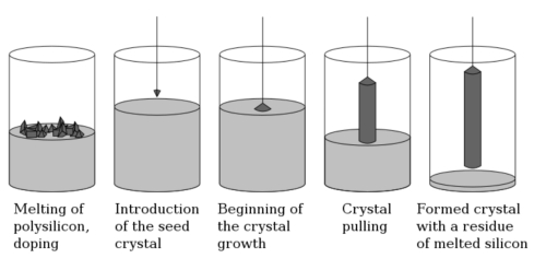
Fig. 2 Principle of Czochralski Method
Vertical Gradient Freezing (VGF) Method
The Vertical Gradient Freezing method, an advanced technique for single-crystal growth, relies on precise temperature gradient control to guide crystal growth. Unlike the Czochralski method, the VGF method is particularly advantageous for producing high-purity materials with fewer lattice defects.
Steps in the VGF Method:
- Preparation of the Melt:
High-purity germanium is placed in a crucible made of heat-resistant materials like quartz or platinum. The material is melted and maintained in a liquid state. - Creating the Temperature Gradient:
A vertical temperature gradient is established, with higher temperatures at the top and lower temperatures at the bottom of the melt. This gradient ensures controlled solidification from the bottom upwards. - Seeding and Growth:
A crystal seed, placed in the lower, cooler region of the melt, initiates crystal growth. As the temperature decreases, the melt solidifies upward, following the seed's structure to form a single crystal. The growth rate is carefully controlled to minimize defects, typically proceeding at a slower rate than the Czochralski method. - Gradual Cooling:
Once the melt solidifies into a single crystal, the temperature is reduced gradually to avoid thermal stress or cracks.
Advantages of the VGF Method:
- High Precision: The stable temperature gradient minimizes defects like dislocations and lattice distortions.
- High Purity: Impurity removal is more effective, making the method ideal for optoelectronic and high-frequency devices.
- Brittle Material Compatibility: Unlike the Czochralski method, the VGF method avoids issues like crystal rupture, making it suitable for brittle materials.
Challenges:
The VGF method requires advanced equipment for precise temperature control, making it costlier. Additionally, its slower crystal growth rate reduces production efficiency, particularly for high-volume manufacturing.
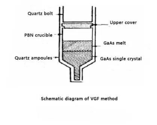
Fig. 3 Schematic Diagram of VGF Method
Comparison and Applications
Both the Czochralski and VGF methods have their merits and limitations. The Czochralski method excels in scalability and efficiency, making it ideal for industries requiring high production volumes. In contrast, the VGF method provides higher-purity crystals with fewer defects, making it suitable for high-end applications like quantum computing, solar cells, and advanced optoelectronics.
Despite its niche role compared to silicon, germanium continues to be indispensable in applications where its unique properties—low bandgap, infrared sensitivity, and high-frequency capabilities—offer distinct advantages. From infrared detectors to high-speed transistors, germanium remains a vital material for the advancement of electronic and optoelectronic technologies.
Conclusion
Germanium, with its exceptional electrical and optical properties, continues to play a pivotal role in advanced electronics and optoelectronics despite challenges in production and scalability. Its unique characteristics, such as a small bandgap, high infrared sensitivity, and compatibility with silicon, make it indispensable for niche applications, including high-frequency electronics, fiber-optic communications, and infrared detection.
Stanford Electronics is a key provider of high-quality germanium materials, supporting these critical applications with reliable material solutions. For more information about Germanium and essential electronic materials, please check our homepage.


 Powder for Li-ion Battery Cathodes")
