
Gallium Arsenide Wafer VS. Silicon Wafer
Introduction
As electronic devices evolve, understanding wafers, chips, semiconductors, and integrated circuits becomes increasingly important. Questions often arise: What is a wafer? What is a chip? How are they related? What materials are used, and what are their advantages and disadvantages? This article explores these questions by comparing gallium arsenide wafers and silicon wafers, offering a clearer perspective on their roles in the semiconductor industry.
Wafers & Chips
What is a wafer?
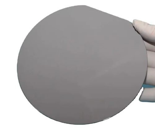
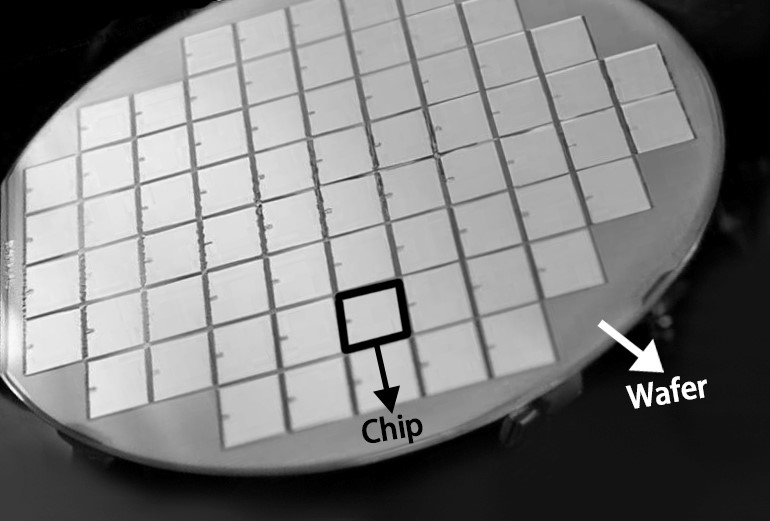
A wafer is a thin slice of semiconductor material used as the substrate for integrated circuits and other electronic devices. Wafers form the foundation of the electronics industry.
What is a chip?
A chip, also known as an integrated circuit (IC), contains multiple electronic circuits embedded in a single piece of semiconductor material. Chips integrate miniaturized transistors and components for various electronic functions.
What is their difference?
The wafer serves as the substrate for the chip, while the chip is embedded into the wafer. Together, they play a vital role in electronic applications.
Gallium Arsenide Wafer vs. Silicon Wafer
Silicon Wafers
Pros:
Silicon remains the dominant choice for wafers due to its cost-effectiveness, making up over 90% of the semiconductor market. Its favorable current and voltage handling capabilities also enable broad application across various technologies.
Cons:
Silicon's brittleness limits its use for large-size wafers, as its crystalline structure makes it prone to cracking. Increasing wafer thickness to reduce breakage raises costs, diminishing silicon's price advantage.
Gallium Arsenide Wafers
Pros:
Gallium arsenide (GaAs) wafers offer notable technical advantages:
- High Electron Mobility: Electrons move faster in GaAs, making it ideal for high-speed telecommunication devices.
- Optoelectronic Properties: GaAs converts electricity into light, enabling applications in laser diodes, optical windows, solar cells, and other optoelectronics.
- Noise Reduction and Temperature Range: GaAs devices have lower noise levels and can operate in broader temperature ranges than silicon-based counterparts.
Cons:
Gallium arsenide wafers also have drawbacks:
- Higher Cost: GaAs is rarer and more expensive than silicon, though its efficiency justifies the price for high-budget applications.
- Oxide Formation: Unlike silicon, GaAs cannot form native oxides for insulation.
- Toxicity Concerns: Arsenic in GaAs requires careful handling and disposal due to its toxicity.
Conclusion
Both wafers and chips are critical to the semiconductor and electronics industries. While silicon wafers are cost-efficient and widely used, gallium arsenide wafers excel in electron mobility, optical properties, and efficiency. Stanford Electronics offers high-quality single-crystal gallium arsenide wafers manufactured using LEC and VGF methods. Visit our homepage for further information.


 Powder for Li-ion Battery Cathodes")
